
4 layers99 × 62 mm

 swpfY/RP-Link4
基于Picoprobe的树莓派pico调试器
RP Link is an open-source printed circuit board by swpfY, from the swpfY/RP-Link repository on GitHub. It is a 2-layer board of 17 × 45.3 mm with 32 parts on 58 nets, routed with 201 tracks and 66 vias.
It is built around the RP2040, W25Q16JVUXIQ and ME6211C33M5G-N, with the TYPE-C 16PF among its other parts. Its parts include 15 capacitors, 8 resistors, 3 ICs, 2 diodes and 2 connectors. It belongs with the RP2040 boards of this library.


原理图在:RP-Link.pdf
实物图在: static/RP-Link_.jpeg
bom表在:bom/ibom.html
genber文件在:genber/
引脚定义如下图:
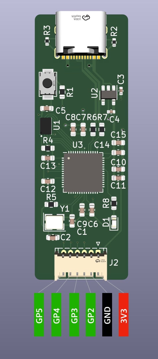
PCB设计参考自:raspberry pi pico 和 EnvOpenPico
生成交互式Bom表单的插件为:InteractiveHtmlBom
picoprobe 可执行文件可以在 Releases 中找到
🤪目前刚入门水平有限,还在学习,后续会继续优化迭代
| Qty | Value | Footprint | References |
|---|---|---|---|
| 9 | 100n | Capacitor_SMD:C_0402_1005Metric | C5, C6, C7, C10, C11, C12, C13, C14, C15 |
| 2 | 1K | Resistor_SMD:R_0402_1005Metric | R1, R5 |
| 2 | 1u | Capacitor_SMD:C_0603_1608Metric | C3, C4 |
| 2 | 1u | Capacitor_SMD:C_0402_1005Metric | C8, C9 |
| 2 | 20p | Capacitor_SMD:C_0402_1005Metric | C1, C2 |
| 2 | 27r | Resistor_SMD:R_0402_1005Metric | R6, R7 |
| 2 | 5.1K | Resistor_SMD:R_0402_1005Metric | R2, R3 |
| 1 | 10K | Resistor_SMD:R_0402_1005Metric | R4 |
| 1 | 470r | Resistor_SMD:R_0402_1005Metric | R8 |
| 1 | Conn_01x06 | Connector_Hirose:Hirose_DF13-06P-1.25DS_1x06_P1.25mm_Horizontal | J2 |
| 1 | Crystal_GND24 | Crystal:Crystal_SMD_3225-4Pin_3.2x2.5mm | Y1 |
| 1 | D_Schottky | Diode_SMD:D_SOD-123F | D2 |
| 1 | LED | LED_SMD:LED_0603_1608Metric | D1 |
| 1 | ME6211C33M5G | Package_TO_SOT_SMD:SOT-23-5 | U2 |
| 1 | RP2040 | Package_DFN_QFN:QFN-56-1EP_7x7mm_P0.4mm_EP3.2x3.2mm | U3 |
| 1 | SKRKAEE020_SMD | Button_Switch_SMD:SKRKAEE020 | SW1 |
| 1 | TYPE-C_16P | Connector_USB:USB_C_Receptacle_XKB_U262-16XN-4BVC11 | J1 |
| 1 | W25Q16JVUX | Package_SON:USON-8_2x3mm_P0.6mm | U1 |


thomaslr/plant-esp32
This directory contains the production files, Pick & Place centroid files (CPL), Bill of Materials (BOM), KiCad design source files, and 3D renders for the Monolithic Onboard SMD Edition of the Plant ESP32 watering…

LastZactionHero/defcon-silent-disco
RP2040-based DEF CON silent disco badge — KiCad project + tooling
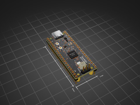
Hanqaqa/Easyduino
Easily dive into different PCB KiCad designs of the most popular microcontroller devboards


FrameworkComputer/InputModules
Reference designs and documentation for the Input Module system in the Framework Laptop 16

It measures 17 × 45.3 mm and has 2 copper layers, 1.6 mm thick.
32 parts, built around the RP2040, W25Q16JVUXIQ, ME6211C33M5G-N and TYPE-C 16PF. The full list of its parts is on this page, with links to each part's symbol and footprint where PCBKit's library has them.
From the swpfY/RP-Link repository on GitHub, at the commit this page was made from: the board is RP-Link.kicad_pcb and its schematic RP-Link.kicad_sch. PCBKit opens the board in the browser, with nothing to install.
Its repository states no licence, so its author keeps all rights: ask swpfY before reusing the design.