2 layers80 × 67 mm
MinisumoV2
LaboratorioGluon/Minisumo-FullMango
Robot minisumo de competición para la OSHWDEM 2026
97 parts1MIT

 SuperTails/16299-balancing-robot
Control PCB for 16299 at CMU
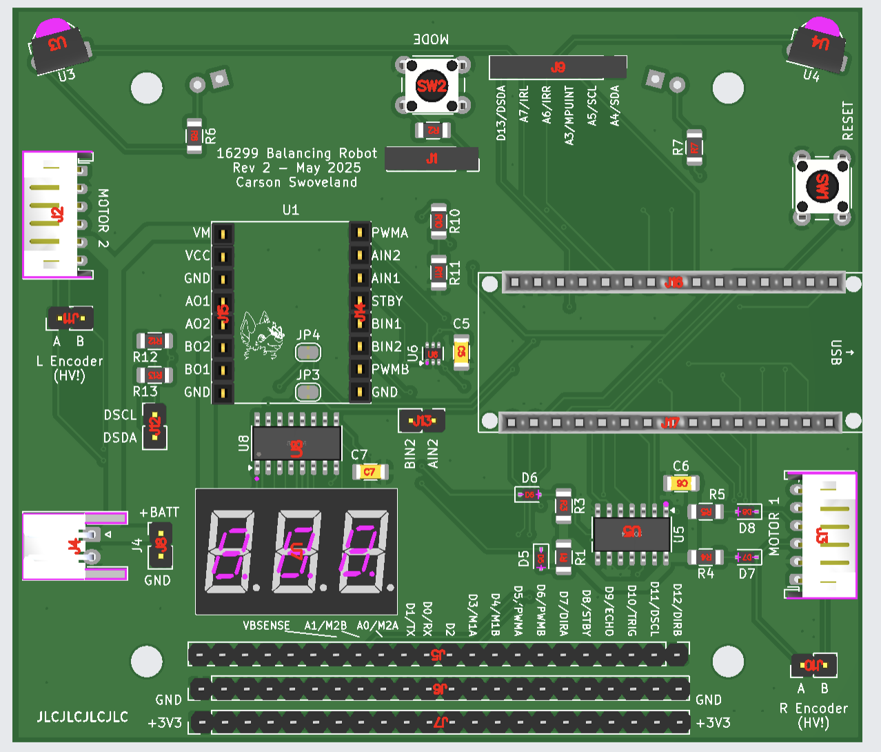
Balancingrobot is an open-source printed circuit board by SuperTails, from the SuperTails/16299-balancing-robot repository on GitHub. It is a 4-layer board of 95 × 82 mm with 50 parts on 70 nets, routed with 494 tracks and 108 vias.
It is built around the ROB-14450, IRM-56384 and 74HC14, with the 74LVC2G14GW, BAT54J and IR204-A-L among its other parts. Its parts include 13 connectors, 11 resistors, 7 ICs, 6 diodes and 3 capacitors. It belongs with the RP2040 and AVR (ATmega, ATtiny) boards of this library.


Updated version of the PCB for 16299.
A submodule is used for some parts, so be sure to clone recursively:
git clone --recursive https://github.com/SuperTails/16299-balancing-robot.gitTo generate the BoM:
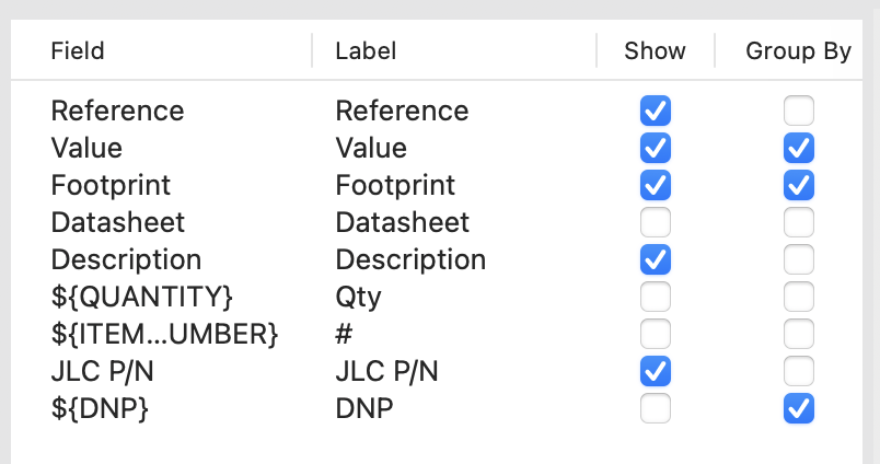
To generate the gerber files:
fab/.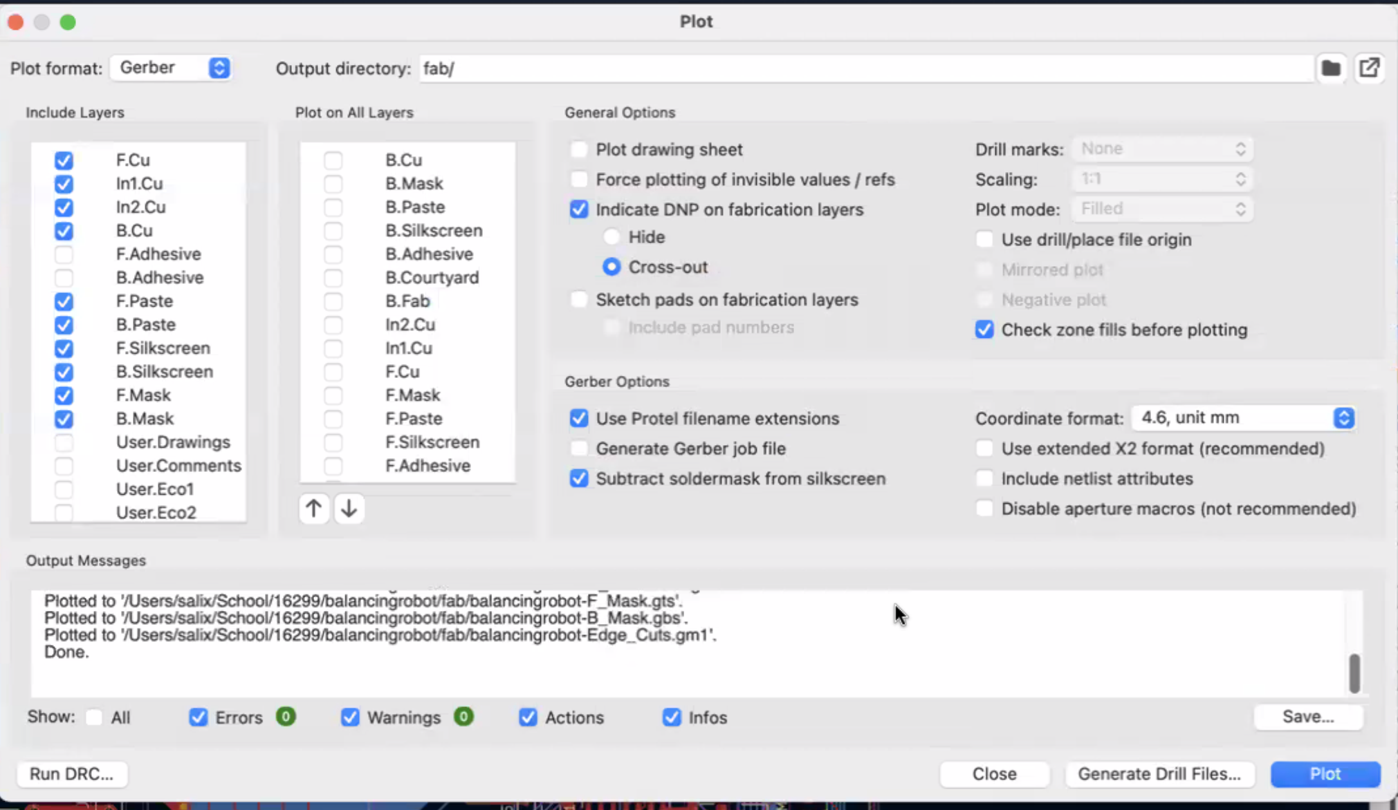
More information for plotting Gerber and Drill files is available on JLC's guide.
To generate the drill files:
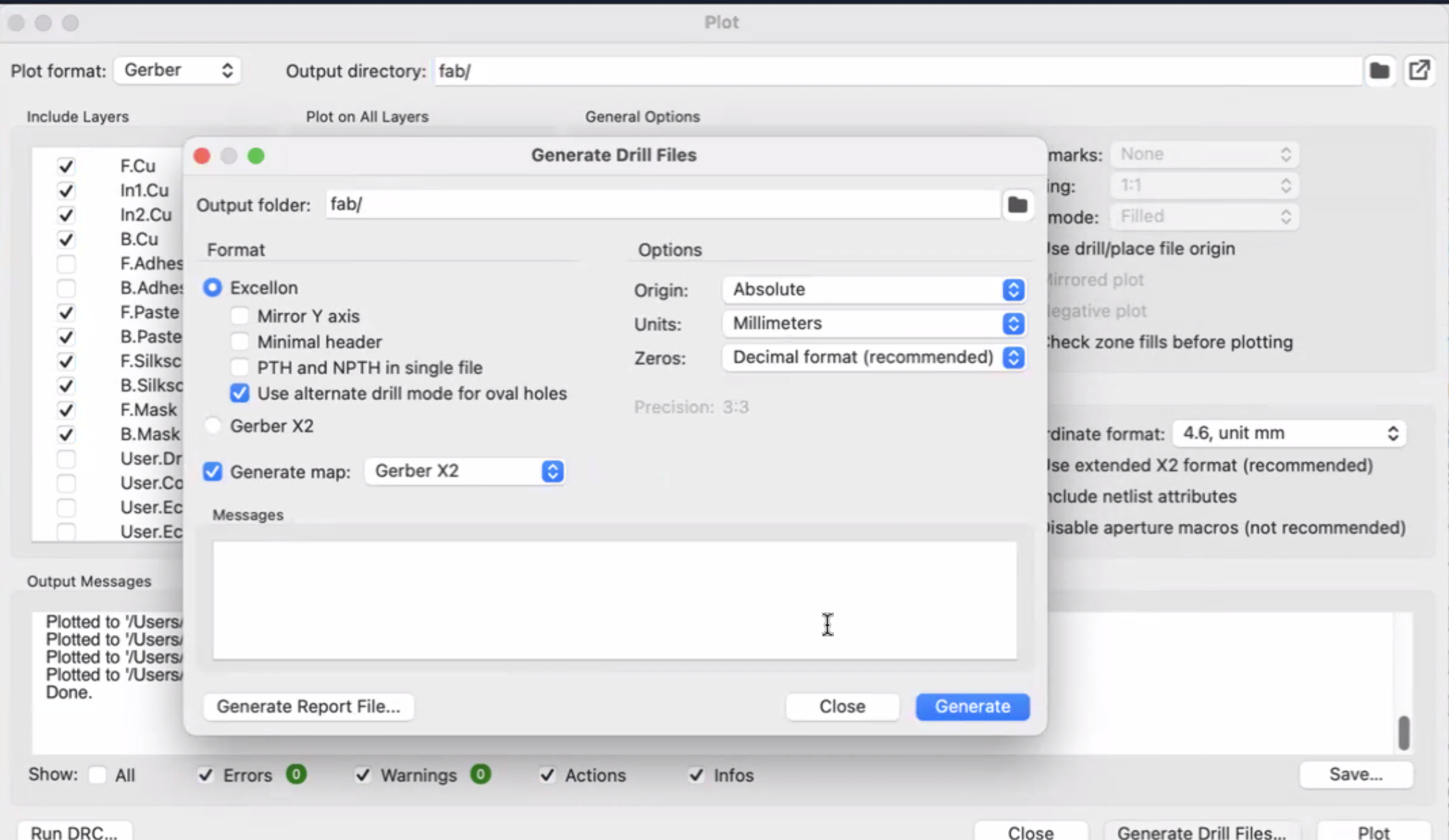
More information for plotting Gerber and Drill files is available on JLC's guide.
To generate the placement files:
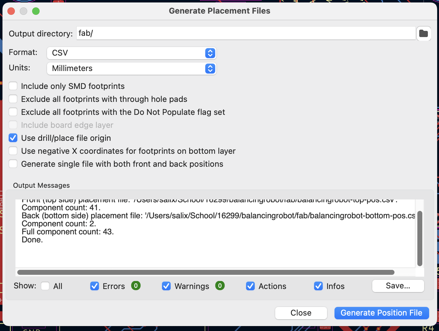
To convert the files into JLC's preferred format, run the format_bom.py script:
python3 format_bom.pyThis will generate fab/bom-jlc.csv and fab/balancingrobot-top-pos-jlc.csv,
which should be used for JLC's PCB assembly options (discussed later).
Zip the fab/ directory and upload it to JLC's website.
Rarely, the file upload can take up to 10 minutes to complete.
Most settings should default correctly, but there are a few changes:



When prompted to "Upload BOM" and "Add CPL file",
upload fab/bom-jlc.csv and fab/balancingrobot-top-pos-jlc.csv.
It may issue a warning that D9 and D10 are not present in the CPL, this is normal and you can continue. D9 and D10 are the IR LEDs which are mounted on the underside of the board, and doing assembly for both top and bottom components makes shipping difficult.
All parts should be selected in the right column and there should be no other errors.
When moving on to placement, JLC may note that "The system detects component that may be offset from the PCB, does it try to automatically align it?" Click cancel on this prompt, as it will displace many of the components to the wrong place.
The through-hole components typically need to be both rotated and dragged to fit; the surface mount components should only be rotated.
Ensure that all surface mount components have the pink dot (pin 1) aligned with the corresponding silkscreen arrow. Some of the SMD components may be upside-down.
There will be four rows of header pins far above the rest of the PCB (shown below); these are the sockets for the Arduino Nano and the motor driver. Be sure to place them as well.
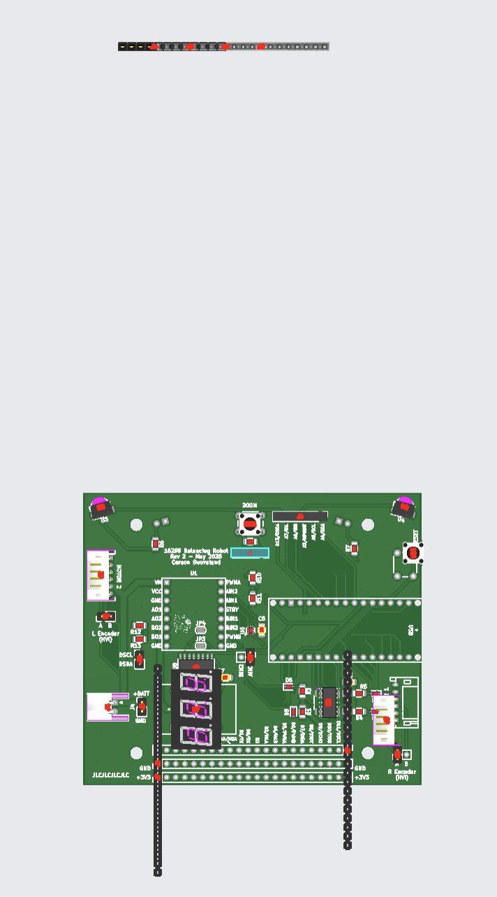
Once placement is finished, the board should appear as shown below:
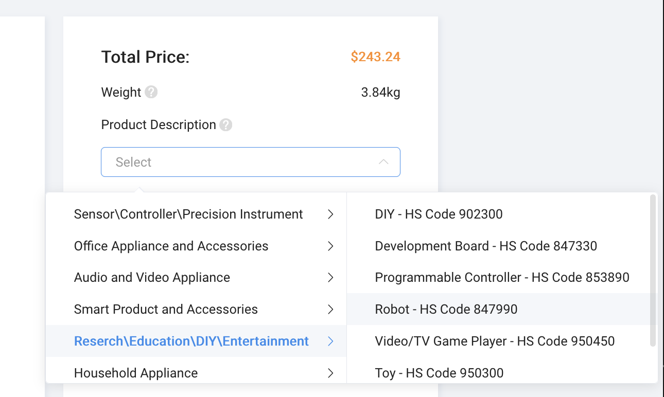
When prompted to select a category for your order, I usually select "Robot", as shown below:
This completes all the placement steps, simply complete the rest of the checkout steps to order the PCB.
After ordering, you may receive an email saying that the footprint of the 7-segment display is incorrect. As long as the decimal point is on the bottom and the pink dot is in the bottom left, reply to the email and say the placement is correct.
| Qty | Value | Footprint | References |
|---|---|---|---|
| 6 | 4.7k | Resistor_SMD:R_1206_3216Metric | R1, R3, R4, R5, R12, R13 |
| 5 | Conn_01x02 | Connector_PinHeader_2.54mm:PinHeader_1x02_P2.54mm_Vertical | J8, J10, J11, J12, J13 |
| 4 | BAT54J | Diode_SMD:D_SOD-323F | D5, D6, D7, D8 |
| 3 | 10nF | Capacitor_SMD:C_1206_3216Metric | C5, C6, C7 |
| 3 | Conn_01x22 | Connector_PinHeader_2.54mm:PinHeader_1x22_P2.54mm_Vertical | J5, J6, J7 |
| 2 | 10k | Resistor_SMD:R_1206_3216Metric | R2, R10 |
| 2 | 1k | Resistor_SMD:R_1206_3216Metric | R6, R7 |
| 2 | Conn_01x06 | Connector_JST:JST_PH_S6B-PH-K_1x06_P2.00mm_Horizontal | J2, J3 |
| 2 | IR204A | LED_THT:LED_D3.0mm_IRBlack | D9, D10 |
| 2 | IRM-56384 | OptoDevice:Vishay_MOLD-3Pin | U3, U4 |
| 2 | SW_Push | Button_Switch_THT:SW_PUSH_6mm | SW1, SW2 |
| 2 | SolderJumper_2_Bridged | Jumper:SolderJumper-2_P1.3mm_Bridged_RoundedPad1.0x1.5mm | JP3, JP4 |
| 1 | 5.6k | Resistor_SMD:R_1206_3216Metric | R11 |
| 1 | 74HC14 | Package_SO:SOIC-14_3.9x8.7mm_P1.27mm | U5 |
| 1 | 74LVC2G14 | Package_TO_SOT_SMD:SOT-363_SC-70-6 | U6 |
| 1 | ARKLED | Custom:ARKLED(Wuxi ARK Tech Elec) SP420361N | U7 |
| 1 | Arduino_Nano_RP2040_Connect_Socket | Arduino:Arduino_Nano_Every_Socket | A1 |
| 1 | Conn_01x02 | Connector_JST:JST_XH_S2B-XH-A-1_1x02_P2.50mm_Horizontal | J4 |
| 1 | Conn_01x04 | Connector_PinSocket_2.54mm:PinSocket_1x04_P2.54mm_Vertical | J1 |
| 1 | Conn_01x06 | Connector_PinHeader_2.54mm:PinHeader_1x06_P2.54mm_Vertical | J9 |
| 1 | LOGO | Custom:salix | G*** |
| 1 | ROB-14450 | Custom:ROB-14451 | U1 |
| 1 | ~ | Package_SO:SOP-16_3.9x9.9mm_P1.27mm | U8 |
The 46 most common of 50 parts.
It measures 95 × 82 mm and has 4 copper layers, 1.6 mm thick.
50 parts, built around the ROB-14450, IRM-56384, 74HC14 and 74LVC2G14GW. The full list of its parts is on this page, with links to each part's symbol and footprint where PCBKit's library has them.
From the SuperTails/16299-balancing-robot repository on GitHub, at the commit this page was made from: the board is balancingrobot.kicad_pcb and its schematic balancingrobot.kicad_sch. PCBKit opens the board in the browser, with nothing to install.
Its repository states no licence, so its author keeps all rights: ask SuperTails before reusing the design.
LaboratorioGluon/Minisumo-FullMango
Robot minisumo de competición para la OSHWDEM 2026

skumlos/bkm-10rlternative
Project aiming to replicate the BKM-10R/11R remote for Sony professional CRT monitors.


Mr-Bossman/SD_Swap
A development tool which swaps an sdcard between a usb3 card reader or a SBC.

mikelawrence/WiFi-Gate-Controller
WiFi enabled Gate Controller Addon to US Automatic Gate Opener

mikelawrence/WiFi-Septic-Controller
WiFi enabled Septic Controller
