6 layers134 × 189 mm

 Studio-Fug/yapnr5
Yet-another-place-and-route engine for PCBs.
Splanc dev is an open-source printed circuit board by Studio-Fug, from the Studio-Fug/yapnr repository on GitHub, published under the AGPL-3.0 licence. It is a 2-layer board of 787 × 7 mm with 79 parts on 71 nets, routed with 1,079 tracks and 165 vias.
Its parts include 27 capacitors, 25 resistors, 11 ICs, 4 transistors and 4 switches.



Yet another place and route engine for printed circuit boards.
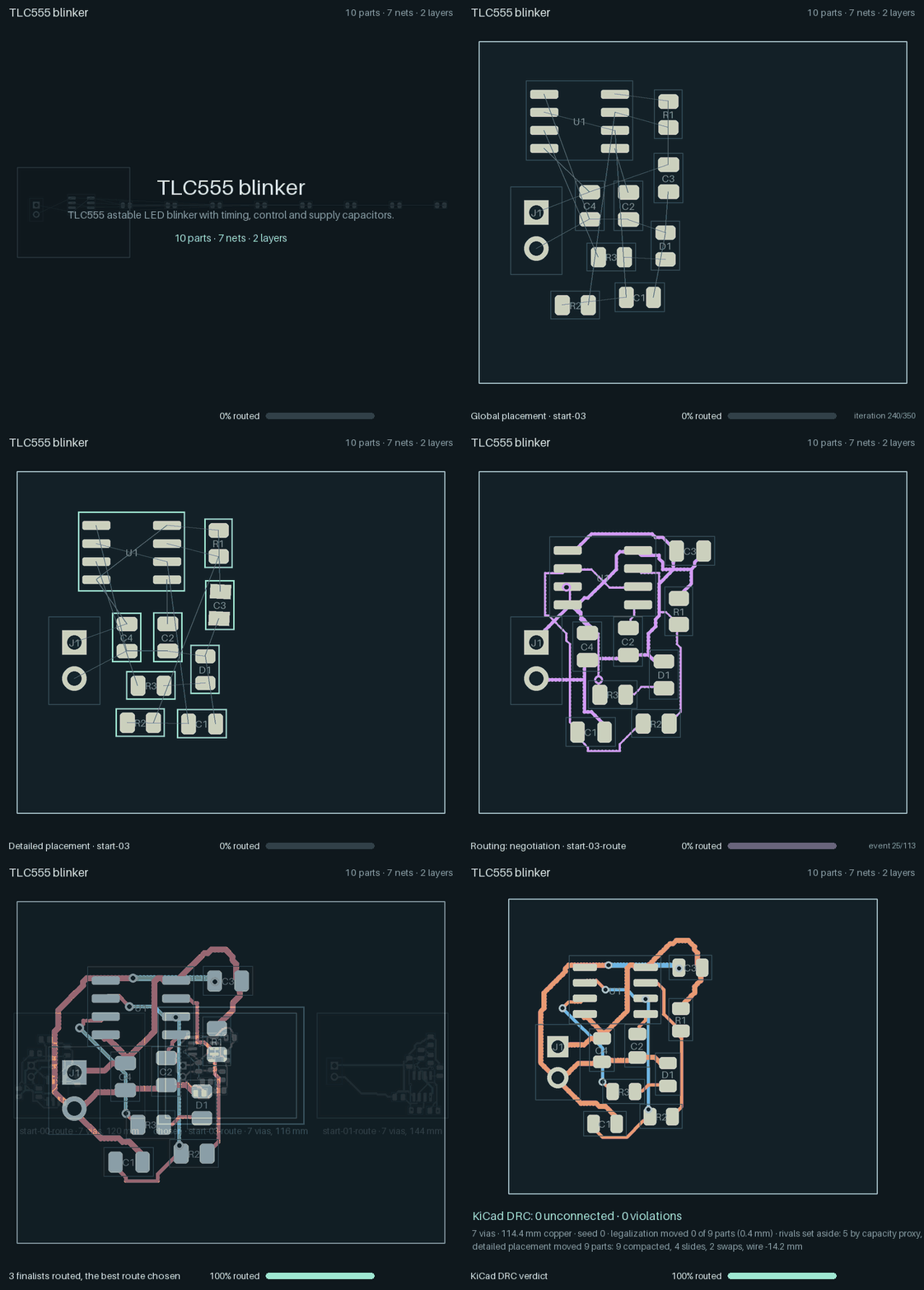
The 555 flasher (a TLC555 astable blinker, 10 parts, 2 layers) from the
regression ladder: from unplaced footprints to 100 % routed, with the
placement starts and routes it was chosen from, then the gloss pass (the copper it replaces in
red, its new copper in green), ending on KiCad's clean DRC verdict. Recorded with the opt-in
compact placement and gloss
(PNR_COMPACT=1, PNR_GLOSS=1; both off by default).
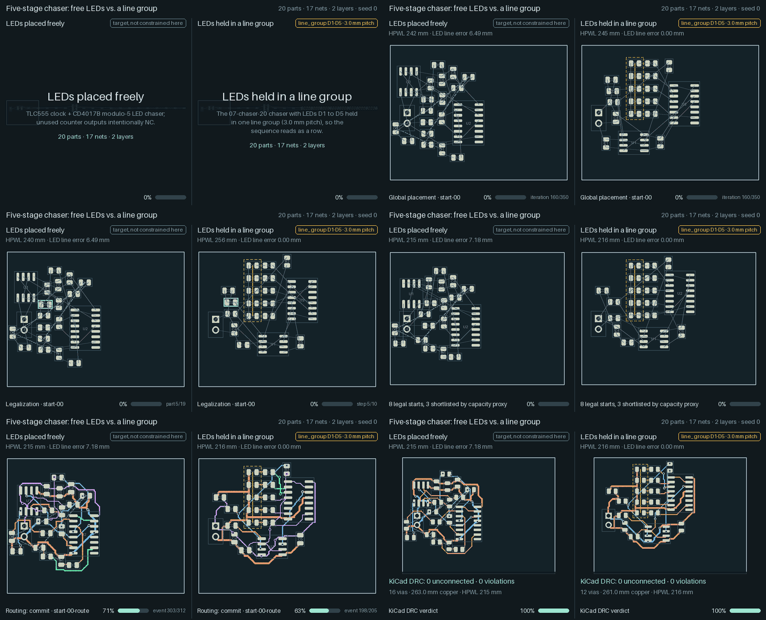
Left: LEDs placed freely. Right: the same chaser with its LEDs held in a line group; compact placement keeps each LED's series resistor flush beside it, and the placer moves and turns the whole row. Both with compact placement and gloss, as above.
yapnr places components and routes copper for KiCad boards. It uses a mechanical, Monte-Carlo-driven search: hierarchical block synthesis, power-first placement, native KiCad routing and DRC in the loop, and electrical contracts (current, pairs, plane access) declared next to the design.
The engine is being migrated here from the Splanc repository,
where it was developed to lay out the Splanc Mini board. The migration plan and progress are in
docs/ and WORKLOG.md.
The papers and open-source projects it builds on are listed in
Foundations and references.
Alpha: this repository holds the build, CI and documentation scaffolding, a command-line stub, the
migration plan, and the engine imported from Splanc at its original
paths under hardware/: its committed history and its newer, uncommitted state
(manifest). The package restructuring follows. KiCad 10 only.
With Bazelisk installed as bazel:
bazel run //:yapnr -- --version   # the CLI
bazel run //:doctor               # environment report
bazel test //...                  # unit tests and repository checks
bazel run //docs:build            # documentation -> docs/site/html/
See DEVELOPERS.md for setup (including the headless KiCad copy on macOS) and CONTRIBUTING.md for the contribution policy.
ghcr.io/studio-fug/yapnr bundles KiCad 10, CPython 3.11 with CPU-only torch, and yapnr, for
linux/amd64 and linux/arm64, so running yapnr needs Docker and nothing else:
docker run --rm ghcr.io/studio-fug/yapnr:edge doctoredge follows main; release tags (X.Y.Z, X.Y, latest) start with v0.1.0. See
docs/containers.md for projects, UID mapping, resource limits and Apple
Silicon, and docs/releases.md for versioning and releases.
Copyright (C) 2026 Kevin Balke. Licensed under the GNU Affero General Public License v3.0 or later
(AGPL-3.0-or-later); see LICENSE. Third-party material is listed in
THIRD_PARTY.md.
Ask your agent “Please use Studio-Fug/yapnr to design X” and have it read
AGENTS.md. Start yapnr agent chat in an interactive container;
the execution guide covers authentication, resource
limits, resumption and the open assembly-validation gates.
| Qty | Value | Footprint | References |
|---|---|---|---|
| 14 | Samsung_CL05B104KO5NNNC:C0402 | C2, C3, C4, C8, C14, C16, C17, C19, C20, C22, C23, C24, C25, C26 | |
| 8 | UNI_ROYAL_0603WAF1002T5E:R0603 | R4, R5, R10, R13, R15, R19, R24, R25 | |
| 4 | XKB_TS_1088_AR02016:SW-SMD_L3.9-W3.0-P4.45 | SW1, SW2, SW3, SW4 | |
| 4 | Samsung_CL21A106KAYNNNE:C0805 | C10, C11, C18, C21 | |
| 4 | UNI_ROYAL_0402WGF1001TCE:R0402 | R1, R9, R14, R18 | |
| 4 | UNI_ROYAL_0402WGF2001TCE:R0402 | R8, R11, R22, R23 | |
| 4 | Samsung_CL05A105KA5NQNC:C0402 | C1, C9, C12, C13 | |
| 3 | Samsung_CL21A226MOQNNNE:C0805 | C5, C6, C7 | |
| 3 | UNI_ROYAL_0402WGF1003TCE:R0402 | R2, R3, R12 | |
| 2 | Changjiang_MMBT3904_RANGE_100_300:SOT-23-3_L2.9-W1.3-P1.90-LS2.4-BR | Q1, Q3 | |
| 2 | Texas_Instruments_SN74LVC1T45DBVR:SOT-23-6_L2.9-W1.6-P0.95-LS2.8-BR | U8, U10 | |
| 2 | Sunlord_SWPA6045S1R0NT:IND-SMD_L6.0-W6.0_SWPA6045S | L2, L3 | |
| 2 | Texas_Instruments_INA226AIDGSR:MSOP-10_L3.0-W3.0-P0.50-LS5.0-BL | U7, U9 | |
| 2 | UNI_ROYAL_0402WGF330JTCE:R0402 | R17, R21 | |
| 2 | Alpha___Omega_AO3401A:SOT-23_L2.9-W1.3-P1.90-LS2.4-BR | Q2, Q4 | |
| 2 | JST_B3B_PH_K_S_LF__SN:CONN-TH_B3B-PH-K-S | CN2, CN3 | |
| 2 | Samsung_CL10A106KP8NNNC:C0603 | C15, C27 | |
| 2 | UNI_ROYAL_0402WGF5101TCE:R0402 | R6, R7 | |
| 2 | UNI_ROYAL_0402WGF0000TCE:R0402 | R16, R20 | |
| 1 | Texas_Instruments_TPS61088RHLR:VQFN-20_L4.6-W3.6-P0.50-BL | U2 | |
| 1 | Microchip_MCP73831T_2ACI_OT:SOT-23-5_L3.0-W1.7-P0.95-LS2.8-BL | U4 | |
| 1 | Korean_Hroparts_TYPE_C_16PIN_2MD_073:USB-C-SMD_TYPE-C-16PIN-2MD-073 | USB1 | |
| 1 | Espressif_Systems_ESP32_C6_WROOM_1_N8:WIRELM-SMD_ESP32-C6-WROOM-1 | U5 | |
| 1 | Analog_Devices_MAX17048G_T10:TDFN-8_L2.0-W2.0-P0.50-BL-EP1.2 | U6 | |
| 1 | Texas_Instruments_TLV62569DBVR:SOT-23-5_L3.0-W1.7-P0.95-LS2.8-BR | U3 | |
| 1 | Sunlord_GZ2012D601TF:L0805 | L1 | |
| 1 | Bosch_BMP280:LGA-8_L2.5-W2.0-P0.65_AMP6127 | U1 | |
| 1 | XKB_PZ254V_12_20P:HDR-TH_20P-P2.54-V-M-R2-C10-S2.54 | H1 | |
| 1 | JST_B2B_PH_K_S_LF__SN:CONN-TH_B2B-PH-K-S | CN1 | |
| 1 | TDK_InvenSense_MPU_6050:QFN-24_L4.0-W4.0-P0.50-BL-EP2.7 | U11 |


espotek-org/Labrador
EspoTek Labrador is a USB device that transforms your PC or smartphone into a fully-featured electronics lab. This repo holds all of the source code!

hackclub/OnBoard
💡 Join 1,000 teenagers and make your first PCB with a $100 grant!

ElectronicCats/Minino
Minino is an original multiprotocol and multiband board made for sniffing, communicating, and attacking IoT devices. It was designed as a mini Cat that integrates the powerful ESP32C6, GPS, microSD and OLED.

strayer/taira-keyboard
A wireless low-profile split mechanical keyboard with 66 keys inspired by the ErgoDash and Corne Chocolate


cnlohr/cnhardware
My dumping grounds for all my kicad projects and random hardware bringup.

It measures 787 × 7 mm and has 2 copper layers, 1.6 mm thick.
79 parts. The full list of its parts is on this page, with links to each part's symbol and footprint where PCBKit's library has them.
From the Studio-Fug/yapnr repository on GitHub, at the commit this page was made from: the board is hardware/pnr/testdata/splanc_dev/splanc_dev.kicad_pcb. PCBKit opens the board in the browser, with nothing to install.
Its repository publishes it under the AGPL-3.0 licence: you may reuse it on that licence's terms (keep the author's notice, and for a copyleft licence share your changes alike).