4 layers90.3 × 26.6 mm

 ste-man/safety-edge-interface
Dual channel 24VDC interface for 8.2kΩ safety edge, with potential free relays and PNP output
Safety edge interface is an open-source printed circuit board by ste-man, from the ste-man/safety-edge-interface repository on GitHub. It is a 2-layer board of 93 × 78 mm with 75 parts on 42 nets, routed with 336 tracks and 117 vias.
It is built around the TBA 1-2411E, SZNUD3160LT1G and 74AHC1G08GW, with the LM393 and SFH6156-2 among its other parts. Its parts include 35 resistors, 9 diodes, 7 capacitors, 7 ICs and 4 transistors. It belongs with the interfaces and adapters boards of this library.


The local Makerspace in my region needed safety edge interfaces for an automatic bi-folding gate. There are lots of sufficient safety edge interface/controllers available to purchase, but they tend to be a bit expensive (for a valid reason) and I decided to make my own.
See rendered image of assembled safety edge interface PCB below:
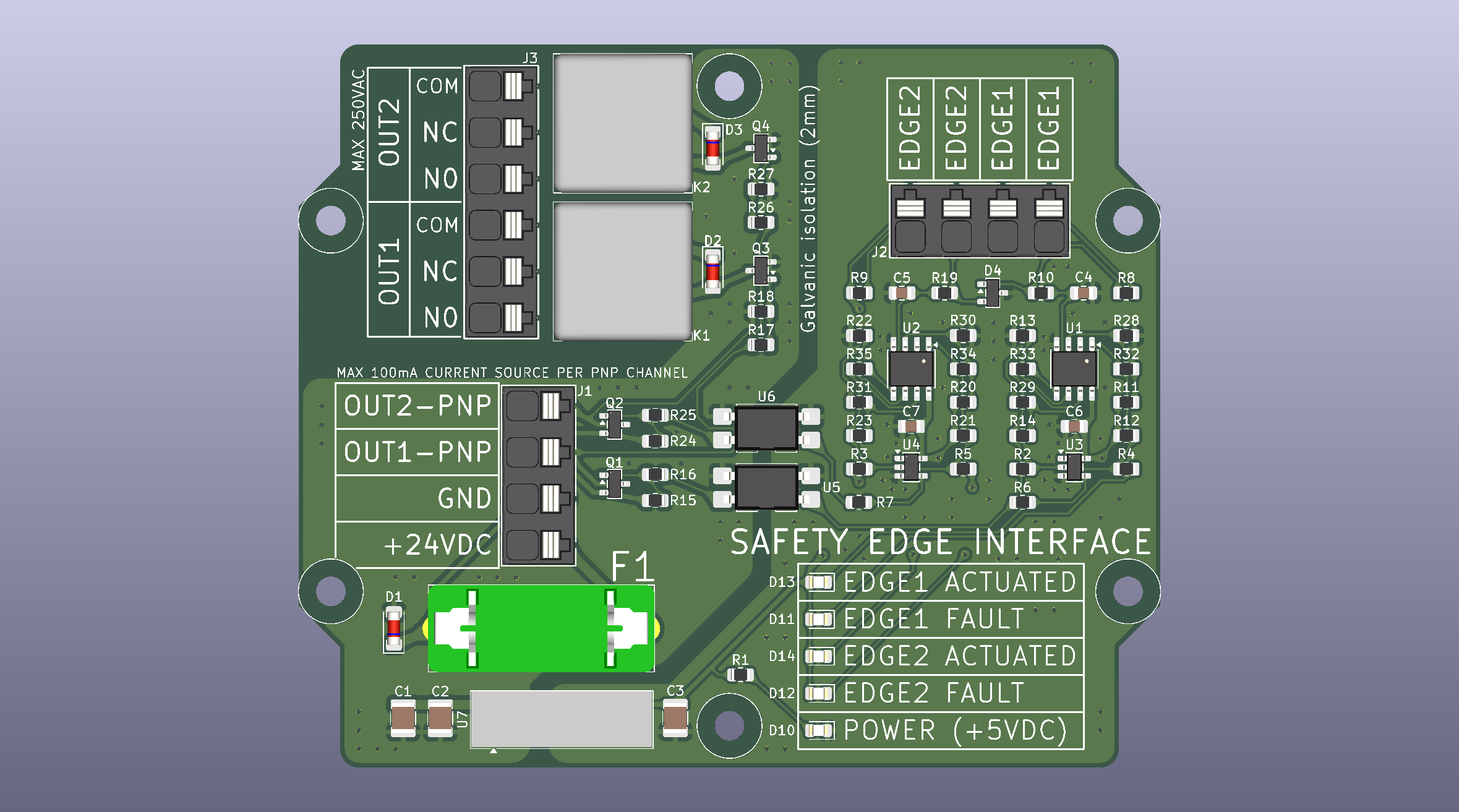
Photos of assembled product is available under directory photos-public.
This safety edge interface monitors the status of two individual safety edge circuits. From google Gemini: A safety edge circuit (also called a pressure-sensitive edge or contact edge circuit) is a fail-safe electric sensing system designed to prevent crushing, shearing, or trapping hazards on automated moving equipment—such as industrial doors, gates, machine guards, and automated guided vehicles (AGVs).
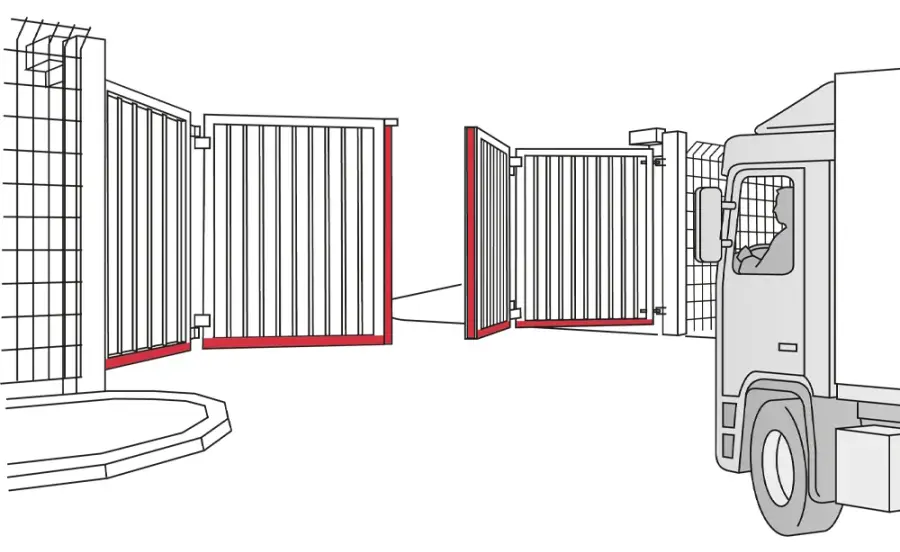
See example of application in image below:
See simplified functional overview below:
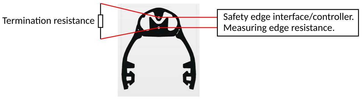
If the interface/controller measures a resistance higher than the termination resistance, the safety edge circuit is considered broken. If the measured resistance is lower than the termination resistance, the edge is considered activated.
If you are located within European Union, your automatic gate and equipment must follow part of the EU Machinery Directive (https://en.wikipedia.org/wiki/Machinery_Directive). There are likely other safety standards applicable as well. No effort has been made to make sure this safety edge controller conforms to any of the standards. A known required functionality is the requirement for monitoring and control of output relay status. This safety edge controller does NOT have active monitoring of the output relays. If the output relay fails welded shut (activated), your safety edge will not be functional.
See exported electrical schematics for a good overview of device full functionality. Electrical schematics and circuit board has been created with software Kicad 10.0.** (https://www.kicad.org/).
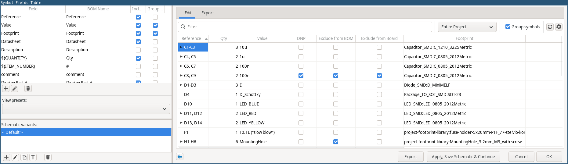
Information with LCSC part numbers (for low cost PCB assembly via JLCPCB) or TME part numbers or Digikey part numbers are included in the KiCad schematic under respective schematic symbol. Full BOM can be viewed via "Tools -> Bulk edit symbol fields" (see screenshot below) or exported via "Tools -> Generate Bill Of Materials".
My version of the printed circuit board was manufactured by JLCPCB. JLCPCB also assembled all "Basic" type (low assembly cost) components available in their store and remaining components were manually purchased and assembled by me in order to minimize the total project cost. Hence the reason for multiple separate distributors. Keep in mind that if you need to change - for example - a LED indicator to an indicator with different brightness, you might need to change the related current limiting resistor to a different value.
Printed circuit board is designed for and verified to fit in enclosure Gainta G221CMF-IP67 (https://www.gainta.com/en/g221cmf-ip67.html). Gainta enclosure G221MF/G221CMF seems to have identical dimensions.
Recommended PCB mounting screws to use with the listed enclosure are included in BOM.
Gainta enclosure G221-IP67/G221/G221C (without mounting flange) seems to have identical internal dimensions, but does include 4 pcs additional M3x5mm insert nuts in the bottom plate. Mounting the PCB in this enclosure would require additional metric type mounting screw.
Fully assembled safety edge interface consumes ~12 mA @ 24 VDC power supply with no safety edges connected and both safety edge channels in FAULT mode. TODO: Measure and add current consumption with relay(s) activated.
A video will be recorded and uploaded to YouTube as soon as the safety edge interface has been installed at the target gate.
Have you detected a mistake somewhere in the project or want to improve it. Send me a pull request or message. My intention is that most of the uploaded and written information should be self explanatory, but feel free to request minor support related to this or similar project(s).
| Qty | Value | Footprint | References |
|---|---|---|---|
| 16 | 10k | Resistor_SMD:R_0805_2012Metric | R10, R12, R13, R14, R15, R16, R17, R18, R19, R21, R22, R23, R24, R25, R26, R27 |
| 6 | MountingHole | project-footprint-library:MountingHole_3.2mm_M3_with-screw | H1, H2, H3, H4, H5, H6 |
| 4 | 15k | Resistor_SMD:R_0805_2012Metric | R11, R20, R29, R31 |
| 4 | 270k | Resistor_SMD:R_0805_2012Metric | R32, R33, R34, R35 |
| 3 | 10u | Capacitor_SMD:C_1210_3225Metric | C1, C2, C3 |
| 3 | 2k | Resistor_SMD:R_0805_2012Metric | R1, R4, R5 |
| 3 | D | Diode_SMD:D_MiniMELF | D1, D2, D3 |
| 2 | 100n | Capacitor_SMD:C_0805_2012Metric | C6, C7 |
| 2 | 1k | Resistor_SMD:R_0805_2012Metric | R6, R7 |
| 2 | 1u | Capacitor_SMD:C_0805_2012Metric | C4, C5 |
| 2 | 20k | Resistor_SMD:R_0805_2012Metric | R28, R30 |
| 2 | 500R | Resistor_SMD:R_0805_2012Metric | R2, R3 |
| 2 | 74AHC1G08 | Package_TO_SOT_SMD:SOT-23-5 | U3, U4 |
| 2 | 8k2 | Resistor_SMD:R_0805_2012Metric | R8, R9 |
| 2 | LED_RED | LED_SMD:LED_0805_2012Metric | D11, D12 |
| 2 | LED_YELLOW | LED_SMD:LED_0805_2012Metric | D13, D14 |
| 2 | LM393 | Package_SO:SO-8_3.9x4.9mm_P1.27mm | U1, U2 |
| 2 | Q_PMOS_GSD | Package_TO_SOT_SMD:SOT-23 | Q1, Q2 |
| 2 | Relay_SPDT | project-footprint-library:relay-9-1415029-1 | K1, K2 |
| 2 | SFH6156 | Package_DIP:SMDIP-4_W9.53mm | U5, U6 |
| 2 | SZNUD3160LT1G | Package_TO_SOT_SMD:SOT-23 | Q3, Q4 |
| 2 | Screw_Terminal_01x04 | project-footprint-library:wago-2086-3104 | J1, J2 |
| 1 | D_Schottky | Package_TO_SOT_SMD:SOT-23 | D4 |
| 1 | Enclosure | project-footprint-library:Gainta-g221mf-enclosure | N1 |
| 1 | LED_BLUE | LED_SMD:LED_0805_2012Metric | D10 |
| 1 | Screw_Terminal_01x06 | project-footprint-library:wago-2086-3106 | J3 |
| 1 | T0.1L ("slow blow") | project-footprint-library:fuse-holder-5x20mm-PTF_77-stelvio-kontek | F1 |
| 1 | TBA1-2411E | project-footprint-library:Converter_DCDC_TRACO_TBA1-xxxxE_Single_THT_modified | U7 |
It measures 93 × 78 mm and has 2 copper layers, 1.6 mm thick.
75 parts, built around the TBA 1-2411E, SZNUD3160LT1G, 74AHC1G08GW and LM393. The full list of its parts is on this page, with links to each part's symbol and footprint where PCBKit's library has them.
From the ste-man/safety-edge-interface repository on GitHub, at the commit this page was made from: the board is ecad/safety-edge-interface/safety-edge-interface.kicad_pcb and its schematic ecad/safety-edge-interface/safety-edge-interface.kicad_sch. PCBKit opens the board in the browser, with nothing to install.
Its repository states no licence, so its author keeps all rights: ask ste-man before reusing the design.

LIV2/A500-2Meg-Chip-ram
An Adapter to retrofit a 2MB agnus into a 1MB Amiga 500/2000

elixpo/elixpo_chapter
Elixpo’s canonical collection for public build-and-release Chapters, bringing open-source software, reproducible research, hardware, and community contributions into one attributable record.


hb020/batterymeter
Handheld Battery AC and Time Domain characterization tool on Attiny series 2


wayri/SPIKE
PCB-focused multiphysics simulation, from board to complete assembly: PI, SI, circuits, thermal, EM/RF and mechanical workflows, with MCAD collaboration and a roadmap toward large-scale coupled assemblies.
