
4 layers99 × 53.3 mm
PSLab
fossasia/pslab-hardware
PSLab Hardware Design and Schematics https://pslab.io
199 parts1.7kApache-2.0

 sqfmi/hexy10
Hexy by SQFMI
Hexy is an open-source printed circuit board by sqfmi, from the sqfmi/hexy repository on GitHub, published under the MIT licence. It is a 2-layer board of 69.3 × 80 mm with 97 parts on 120 nets, routed with 469 tracks and 98 vias.
It is built around the WS2812B. It belongs with the lEDs and displays and home automation and IoT boards of this library.
Inspired by Mukesh Sankhla's HexMatrix project, this is a smaller version using 96 3.5x3.5MM RGB LEDs (WS2812B-MINI)
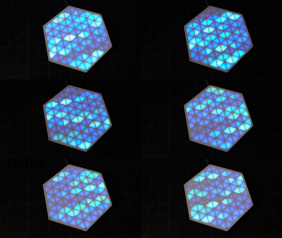
All KiCad design files under MIT license
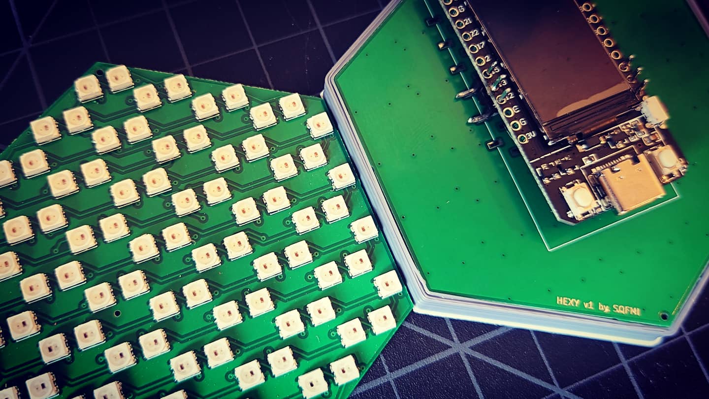
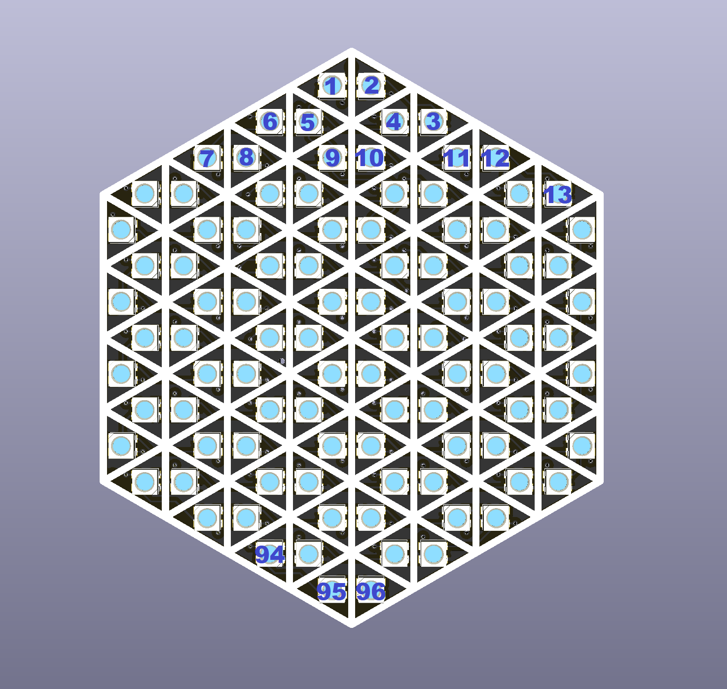
The LEDs are laid out in a zigzag pattern:
We used the FastLED library v3.3
For best visual results, 3D print the seperator grid hexy-frame.stl to keep the light from bleeding over. You will also need a piece of paper/acrylic glued on top to diffuse the light so each triangle cell looks nice and crisp hexy-diffusion.dxf
| Qty | Value | Footprint | References |
|---|---|---|---|
| 96 | WS2812B | hexy:WS2812B-MINI | D1, D2, D10, D11, D12, D13, D14, D15, D16, D17, D18, D19, D20, D21, D22, D23 +80 |
| 1 | TTGO_T-DISPLAY | hexy:TTGO_T-DISPLAY_SMD | TTGO T-DISPLAY |
It measures 69.3 × 80 mm and has 2 copper layers, 1.6 mm thick.
97 parts, built around the WS2812B. The full list of its parts is on this page, with links to each part's symbol and footprint where PCBKit's library has them.
From the sqfmi/hexy repository on GitHub, at the commit this page was made from: the board is hexy.kicad_pcb. PCBKit opens the board in the browser, with nothing to install.
Its repository publishes it under the MIT licence: you may reuse it on that licence's terms (keep the author's notice, and for a copyleft licence share your changes alike).
fossasia/pslab-hardware
PSLab Hardware Design and Schematics https://pslab.io

FrameworkComputer/ExpansionCards
Reference designs and documentation to create Expansion Cards for the Framework Laptop


PrintersForAnts/Micron
If you want to purchase full kits there are 3 available (Kits are slowly updating to R1 hardware just make sure to double check the included hardware in your kit and if you have any questions reach out in the discord)


