
2 layers100 × 74 mm

 SoCXin/nRF528113
L2:Nordic BLE 5.2 SoC
NRF52811 PCB is an open-source printed circuit board by SoCXin, from the SoCXin/nRF52811 repository on GitHub. It is a 4-layer board of 55.4 × 30.5 mm with 27 parts on 23 nets, routed with 139 tracks and 9 vias.
It is built around the TPS73633DBV. Its parts include 10 capacitors, 8 connectors, 2 resistors, 2 ICs and 2 diodes. It belongs with the radio and wireless boards and the nRF52 and nRF5x boards of this library.

nRF52811 Bluetooth 5.1 Direction Finding SoC with comprehensive protocol support. the 4th addition to the nRF52 Series platform.
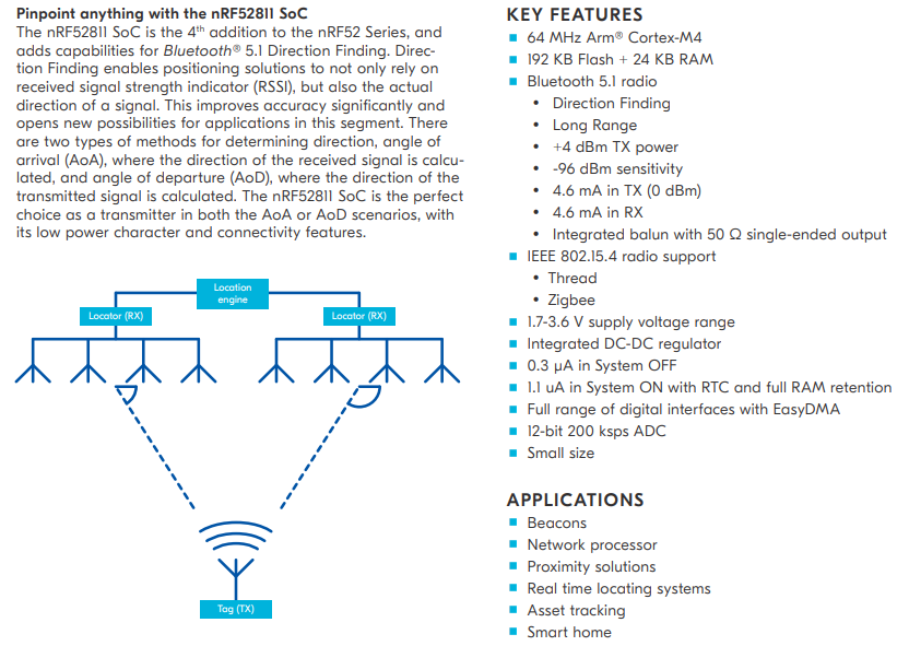
nRF52811 支持BLE 5.2
| Qty | Value | Footprint | References |
|---|---|---|---|
| 3 | 100nF | Capacitor_SMD:C_0805_2012Metric_Pad1.15x1.40mm_HandSolder | C1, C2, C5 |
| 2 | 12pF | Capacitor_SMD:C_0805_2012Metric_Pad1.15x1.40mm_HandSolder | C9, C10 |
| 2 | R_Small | Resistor_SMD:R_0805_2012Metric_Pad1.15x1.40mm_HandSolder | R1, R2 |
| 1 | 0.8pF | Capacitor_SMD:C_0805_2012Metric_Pad1.15x1.40mm_HandSolder | C8 |
| 1 | 100pF | Capacitor_SMD:C_0805_2012Metric_Pad1.15x1.40mm_HandSolder | C6 |
| 1 | 1uF | Capacitor_SMD:C_0805_2012Metric_Pad1.15x1.40mm_HandSolder | C4 |
| 1 | 3.9nH | Inductor_SMD:L_0805_2012Metric_Pad1.15x1.40mm_HandSolder | L1 |
| 1 | 32MHz | Crystal:Crystal_SMD_3225-4Pin_3.2x2.5mm_HandSoldering | Y1 |
| 1 | 4.7uF | Capacitor_SMD:C_0805_2012Metric_Pad1.15x1.40mm_HandSolder | C3 |
| 1 | Antenna_Shield | RF_Antenna:Texas_SWRA117D_2.4GHz_Left | AE1 |
| 1 | BLE LED | LED_SMD:LED_0805_2012Metric_Pad1.15x1.40mm_HandSolder | D2 |
| 1 | Conn_01x08 | Connector_PinSocket_2.54mm:PinSocket_1x08_P2.54mm_Vertical | J4 |
| 1 | JST | Connector_JST:JST_EH_S2B-EH_1x02_P2.50mm_Horizontal | J2 |
| 1 | Mounting_1 | MountingHole:MountingHole_2.2mm_M2_DIN965_Pad | J5 |
| 1 | Mounting_2 | MountingHole:MountingHole_2.2mm_M2_DIN965_Pad | J6 |
| 1 | Mounting_3 | MountingHole:MountingHole_2.2mm_M2_DIN965_Pad | J7 |
| 1 | Mounting_4 | MountingHole:MountingHole_2.2mm_M2_DIN965_Pad | J8 |
| 1 | N.C. | Capacitor_SMD:C_0805_2012Metric_Pad1.15x1.40mm_HandSolder | C7 |
| 1 | Power LED | LED_SMD:LED_0805_2012Metric_Pad1.15x1.40mm_HandSolder | D1 |
| 1 | SWD | Connector_PinHeader_2.54mm:PinHeader_1x04_P2.54mm_Vertical | J1 |
| 1 | TPS73633DBV | Package_TO_SOT_SMD:SOT-23-5_HandSoldering | U1 |
| 1 | USB_B_Micro | Connector_USB:USB_Micro-B_Amphenol_10103594-0001LF_Horizontal | J3 |
| 1 | nRF52811-QFN32 | Package_QFP:LQFP-32_5x5mm_P0.5mm | U2 |
It measures 55.4 × 30.5 mm and has 4 copper layers, 1.6 mm thick.
27 parts, built around the TPS73633DBV. The full list of its parts is on this page, with links to each part's symbol and footprint where PCBKit's library has them.
From the SoCXin/nRF52811 repository on GitHub, at the commit this page was made from: the board is src/hardware/nRF52811_PCB.kicad_pcb. PCBKit opens the board in the browser, with nothing to install.
Its repository states no licence, so its author keeps all rights: ask SoCXin before reusing the design.

FeruzTopalov/eleph
GPS-based local relative navigation system for group of up to 6 members


fsnitz/CcSoM
An open source system on chip based on the GateMate FPGA from Cologne Chip (Supports: CCGM1A1 & CCGM1A2)


hanebefl/wandfernsprecher-hw
GSM conversion for a old German Wandfernsprecher telephone

Volkov997/pen-card
RF Pentesting tool, but small enough for your wallet. Features: Wifi & Bluetooth, NFC, IR, (Sub Ghz, Planned)