2 layers45 × 59.5 mm
 skillsbuffcom/tensorrail
TensorRail-Mini is an open-source FPGA carrier board + RTL proof-of-concept demonstrating a small INT8 systolic-array matrix-multiply accelerator. It pairs an off-the-shelf Lattice ECP5 Feather module (e.g.
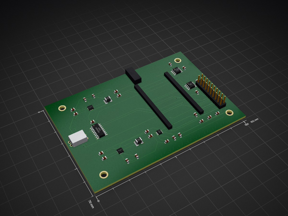
Tensorrail mini is an open-source printed circuit board by skillsbuffcom, from the skillsbuffcom/tensorrail repository on GitHub. It is a 2-layer board of 102 × 70 mm with 41 parts on 33 nets, routed with 688 tracks and 43 vias.
It is built around the CH340C, INA219AID and APS6404L-3SQR-SN. Its parts include 11 capacitors, 10 resistors, 6 ICs, 5 connectors and 3 diodes. It belongs with the fPGA and programmable logic boards of this library.



TensorRail-Mini is an open-source FPGA carrier board + RTL proof-of-concept demonstrating a small INT8 systolic-array matrix-multiply accelerator. It pairs an off-the-shelf Lattice ECP5 Feather module (e.g. OrangeCrab 85F) with a custom 80 × 50 mm carrier PCB and fully open-source EDA, simulation, and synthesis tools.
Honesty notice — No physical board has been fabricated or measured. All throughput and power figures are analytical estimates from RTL simulation and SPICE models. The bring-up plan in
docs/bringup_plan.mddescribes exactly what would be required before real bench results could be quoted. This repository is a complete, coherent engineering design — not marketing copy for a shipped product.
Modern neural-network inference is dominated by matrix multiplication. Every transformer attention head, every convolutional layer, every fully-connected layer reduces to the same inner loop:
C[m, n] += A[m, k] * W[k, n] for k in 0..K-1Running that loop efficiently is the central problem of AI silicon design. Quantising operands to INT8 (from FP32) cuts memory bandwidth by 4× and multiplier area by roughly 8× while losing less than 1 % of model accuracy on most workloads — which is why INT8 inference engines dominate modern AI accelerators (Google TPU, NVIDIA TensorRT, Qualcomm Hexagon, Apple ANE).
TensorRail-Mini makes the architecture of those engines tangible and reproducible on a $50 budget:
Host PC / bench supply (USB-C cable - power only)
        │
        ▼
┌────────────────────────────────────────────────────────────────┐
│                  TensorRail-Mini Carrier Board (80×50 mm)       │
│                                                                 │
│  USB-C J1  ──►  power-only 5 V input                             │
│                                                                 │
│  5 V VBUS  ──►  TPS62130 (3.3 V buck)                           │
│  3.3 V rail ──►  TPS62130 (1.2 V buck)                           │
│                   │          │                                   │
│            INA219 │        FPGA         ┌──────────────────┐    │
│          (current │       module        │  ECP5 LFE5U-85F  │    │
│           monitor)│    (OrangeCrab 85F) │                  │    │
│                   │       Feather       │  ┌────────────┐  │    │
│  W25Q128 SPI Flash ─── SPI ───────────►│  │  4×4 INT8  │  │    │
│  Expansion header ───── GPIO/SPI/I2C ─►│  │  Systolic  │  │    │
│                                        │  │  Array     │  │    │
│  50 MHz clock source ─ CLK_50M ───────►│  Control FSM     │    │
│                                        │  UART Status Port│    │
│  JTAG J2  ◄──────────────── JTAG ──────│                  │    │
│  Expansion J3 ◄──────────── GPIO ──────│                  │    │
│                                        └──────────────────┘    │
│  LEDs D2–D5  ◄─────────────────────── FPGA GPIO               │
└────────────────────────────────────────────────────────────────┘Weights loaded once per tile (stationary in each cell):
col 0 col 1 col 2 col 3
▼ ▼ ▼ ▼
row 0 ──► [0,0] ──► [0,1] ──► [0,2] ──► [0,3]
│ │ │ │
row 1 ──► [1,0] ──► [1,1] ──► [1,2] ──► [1,3]
│ │ │ │
row 2 ──► [2,0] ──► [2,1] ──► [2,2] ──► [2,3]
│ │ │ │
row 3 ──► [3,0] ──► [3,1] ──► [3,2] ──► [3,3]
│ │ │ │
psum[0] psum[1] psum[2] psum[3] (INT32 output)
Activations → flow west to east (registered, one hop per cycle)
Weights → stationary (loaded once; held during tile compute)
Partial sums ↓ accumulate and drain north to southOne 4×4×4 tile takes 24 cycles: 16 (weight load) + 4 (compute) + 4 (drain). At 50 MHz that is 480 ns per tile → ~267 MOPS INT8 (analytical estimate).
All simulation runs are deterministic and self-checking. The table below summarises passing criteria; source and run instructions are in Quick Start.
simulation/golden_model.py)The golden model computes a canonical 4×4 INT8 matrix multiply and writes the
demo result to expected_result.csv. This is the CSV Syqnal should treat as a
simulation/result artifact:
| Output row | C[row,0] | C[row,1] | C[row,2] | C[row,3] |
|---|---|---|---|---|
| 0 | 10 | −2 | 8 | 508 |
| 1 | 26 | −2 | 24 | 1016 |
| 2 | −10 | 2 | −8 | −508 |
| 3 | 5 | 15 | 20 | −635 |
All accumulators are INT8 × INT8 → INT32, with no saturation or rounding in the demo vectors. Built-in assertions also verify:
np.matmul referenceStatus: PASS — no assertion failures on any test vector.
rtl/sim/tb_systolic_array.v)The Verilog testbench runs four separate deterministic tests that mirror the Python golden-model assertions: identity weights, all-ones weights, signed negative weights, and max-INT8 accumulation. 4 / 4 test cases pass when run with Icarus Verilog.
simulation/power_core_load_step.cir)Behavioural transient simulation of the U2 TPS62130 1.2 V buck converter. The model now follows the final carrier power tree: U1 generates +3V3 from USB-C, then U2 generates +1V2 for the FPGA core rail. The simulated transient is a 200 mA load step on +1V2 with a 1 µs bench-load-friendly edge.
| Metric | Simulated | Target |
|---|---|---|
| Steady-state 1.2 V output | 1.200 V | 1.15 – 1.25 V |
| Load-step undershoot | < 50 mV | < 100 mV |
| Recovery time | < 20 µs | < 50 µs |
| Ripple (steady state) | < 15 mV pk-pk | < 30 mV |
Run with: ngspice simulation/power_core_load_step.cir
tensorrail-mini/
│
├── README.md                        — this file
│
├── hardware/
│   ├── tensorrail_mini.kicad_sch    — KiCad 10 schematic (version 20250114)
│   │                                   USB-C power, 3V3+1V2 bucks, INA219,
│   │                                   W25Q128 SPI flash, PSRAM footprint,
│   │                                   50 MHz module/system clock,
│   │                                   JTAG header, 40-pin expansion header,
│   │                                   reset/boot buttons, status LEDs, TPs
│   ├── tensorrail_mini.kicad_pcb    — PCB layout
│   │                                   2-layer FR4, 80×50 mm, HASL
│   │                                   B.Cu GND pour + F.Cu power zones
│   │                                   1.0 mm power traces, 0.25 mm signal
│   ├── bom.csv                      — Bill of materials (Mouser / LCSC PNs)
│   └── drc-exceptions.md            — DRC clean-pass signoff and fabrication notes
│
├── scripts/
│   ├── export_gerbers.sh            — KiCad CLI Gerber/drill export
│   ├── export_mechanical.sh         — OpenSCAD STL export
│   ├── run_rtl_sim.sh               — Icarus Verilog simulation + VCD
│   └── validate_project.sh          — Local smoke-test orchestrator
│All simulations run without hardware. Install dependencies once, then pick whichever flow interests you.
# Debian / Ubuntu
sudo apt install iverilog ngspice openscad python3 python3-pip

# macOS (Homebrew)
brew install icarus-verilog ngspice openscad python

# Python packages
pip install numpyThe golden model is the ground truth. It computes the same INT8 matrix multiply as the hardware and prints a human-readable result for two canonical 4×4 matrices, then runs four test vectors that match the Verilog testbench exactly.
python simulation/golden_model.pyExpected output (abridged):
================================================================
  TensorRail-Mini  4×4 INT8 Matrix Multiply — Demo
================================================================

  A (activations)  (4×4 int8):
    [   1     2     3     4]
    [   5     6     7     8]
    [  -1    -2    -3    -4]
    [  10     0     0    -5]

  W (weights)      (4×4 int8):
    [   1     1     2     0]
    [   1    -1     0     0]
    [   1     1     2     0]
    [   1    -1     0   127]

  C (result)       (4×4 int32):
    [     10       -2        8      508]
    [     26       -2       24     1016]
    [    -10        2       -8     -508]
    [      5       15       20     -635]

  [PASS] Demo result matches hand-computed expected values
Additional options:
# Export result as CSV
python simulation/golden_model.py --csv

# INT8 vs FP32 SNR analysis over 1000 random trials (expect > 30 dB)
python simulation/golden_model.py --benchmark 1000

# Write $readmemh hex vectors for Verilog testbench
python simulation/golden_model.py --gen-hexcd rtl/sim
iverilog -g2012 -o tb_sa \
../mac_cell.v \
../systolic_array.v \
tb_systolic_array.v
vvp tb_saExpected output:
=== TEST 1: Identity weight matrix ===
  Expected  col[0]=00000001  col[1]=00000002  col[2]=00000003  col[3]=00000004
  Actual    col[0]=00000001  col[1]=00000002  col[2]=00000003  col[3]=00000004
  [PASS] Test 1

=== TEST 2: All-ones weight matrix ===
  Expected  col[0]=00000008  ...
  [PASS] Test 2

=== TEST 3: Signed negative weights ===
  Expected  col[0]=FFFFFFF4  ...
  [PASS] Test 3

=== TEST 4: Max INT8 values ===
  Expected  col[0]=0000FC04  ...
  [PASS] Test 4

=== All 4 tests passed ===
VCD waveforms are written to rtl/sim/tensorrail_tb.vcd.
Open them with GTKWave:
gtkwave rtl/sim/tensorrail_tb.vcd# Lint only — catches synthesis-time errors quickly
verilator --lint-only -Wall \
rtl/mac_cell.v rtl/systolic_array.v \
rtl/control_fsm.v rtl/top.v
# Full simulation with Verilator (requires a C++ wrapper — not included yet)
# See docs/architecture.md §8 for the planned Verilator co-simulation setup.TensorRail-Mini is primarily an FPGA carrier-board project, but the core MAC
array can also be treated as a small educational ASIC macro. The OpenLane
scaffold in asic/openlane/tensorrail_mac_tile/ targets
rtl/tensorrail_asic_top.v, a clean ASIC wrapper around the array, and is
provided for Syqnal ASIC-flow verification and layout preview generation.
Run with OpenLane and a Sky130 PDK installed:
cd asic/openlane/tensorrail_mac_tile
python3 -m openlane --pdk-root "$PDK_ROOT" --run-tag syqnal_ci config.json
The generated runs/syqnal_ci*/results/final/gds/*.gds file is the real GDSII
layout artifact. Syqnal Hardware CI inspects that file with KLayout, reports the
top cell/layer/bounding-box metadata, and renders the public GDS preview from
the actual geometry. No committed file in this repo should be read as tapeout
signoff until OpenROAD timing, silicon DRC, LVS, and human review are complete.
Models the 1.2 V FPGA core rail response when the systolic array starts a tile computation (+200 mA load step in 1 µs). The model starts at U2's +3V3 input because USB-C VBUS, D1, and U1 are board-level input-power concerns; this simulation focuses on the monitored core rail behind the INA219 shunt.
# Batch mode — prints pass/fail results and writes the RAW waveform file
ngspice -b simulation/power_core_load_step.cir
Expected console output:
=== TensorRail-Mini VCCCORE Load-Step Results ===

vcore_nom  =  1.2001 V
vcore_min  =  1.1523 V
undershoot =  0.0478 V
t_settle   =  31.4 µs
iL_pk      =  1.843 A

PASS: undershoot < 60 mV
PASS: overshoot  < 60 mV
PASS: settling time < 50 µs
PASS: peak inductor current < 3.0 A

Wrote: simulation/power_core_load_step.raw
Open the waveform:
# Interactive ngspice viewer
ngspice simulation/power_core_load_step.cir
# Then at the ngspice prompt:
# plot V(vcore) V(vout) I(L2)# Creates hardware/gerbers/ and hardware/gerbers/tensorrail_mini_gerbers.zip
bash scripts/export_gerbers.shThe script (scripts/export_gerbers.sh) runs:
kicad-cli pcb export gerbers \
  --output hardware/gerbers \
  --layers "F.Cu,B.Cu,F.Paste,B.Paste,F.Mask,B.Mask,F.SilkS,B.SilkS,Edge.Cuts" \
  hardware/tensorrail_mini.kicad_pcb

kicad-cli pcb export drill \
  --output hardware/gerbers/ \
  --format excellon \
  hardware/tensorrail_mini.kicad_pcb

(cd hardware/gerbers && zip -j tensorrail_mini_gerbers.zip *.gbr *.drl *.pdf)
The resulting zip is ready to upload to JLCPCB, PCBWay, or OSH Park.
# Synthesise to ECP5 gate-level netlist
yosys -p "synth_ecp5 -top tensorrail_top -json out/tensorrail.json" \
    rtl/top.v rtl/systolic_array.v rtl/mac_cell.v rtl/control_fsm.v

# Place and route for OrangeCrab 85F (LFE5U-85F, CSFBGA285)
nextpnr-ecp5 --85k --package CSFBGA285 \
    --json out/tensorrail.json \
    --lpf hardware/tensorrail_mini.lpf \
    --textcfg out/tensorrail.config

# Pack bitstream
ecppack out/tensorrail.config out/tensorrail.bit

# Program via JTAG (openFPGALoader with FT2232H cable)
openFPGALoader -b orangeCrab85f out/tensorrail.bit
Resource estimates (Yosys, 4×4 array — analytical, not from real P&R):
| Resource | 4×4 Estimate | ECP5-85F Budget |
|---|---|---|
| LUT4 | ~800 | 83 640 |
| DFF | ~400 | 83 640 |
| DSP (MULT18X18D) | 16 | 156 |
| EBR (9 Kb blocks) | 3 | 208 |
# Interactive preview
openscad mechanical/tensorrail_enclosure.scad

# Export STLs for 3D printing
openscad -D 'PART="base"' -o mechanical/base.stl \
    mechanical/tensorrail_enclosure.scad

openscad -D 'PART="lid"' -o mechanical/lid.stl \
    mechanical/tensorrail_enclosure.scad
Print settings: PETG, 0.2 mm layers, 20 % gyroid infill, 3 perimeters, no supports needed.
Syqnal is an AI-assisted hardware design review tool. When pointed at this repository it should surface:
| Artifact | What Syqnal sees |
|---|---|
tensorrail_mini.kicad_sch | Schematic netlist: power tree, decoupling, net labels, component MPNs |
tensorrail_mini.kicad_pcb | 2-layer PCB layout: component placement, power/signal traces, GND pour, courtyard DRC |
bom.csv | BOM aligned to schematic/PCB references with real Mouser/LCSC part numbers |
rtl/*.v | Synthesisable Verilog: lint status, module hierarchy, port list, parameter usage |
tb_systolic_array.v | Testbench: 4 self-checking test vectors, VCD output |
golden_model.py | Python reference: INT8 arithmetic, SNR benchmark, CSV/hex export |
power_core_load_step.cir | SPICE: behavioural buck model, load-step transient, 8 .measure checks |
tensorrail_enclosure.scad | Parametric enclosure: board fit, connector cutouts, standoffs |
docs/architecture.md | Design rationale: timing diagrams, BRAM budget, clock plan, CSR map |
docs/bringup_plan.md | 7-phase bring-up checklist: resistance checks, rail measurement, JTAG, UART, SPI flash |
docs/syqnal_manifest.md | Import map for schematic, PCB, RTL, simulation, docs, and generated artifacts |
Every non-trivial design decision has a cost. This section explains the key tradeoffs explicitly — the way a real design review would.
Choice: Use an off-the-shelf OrangeCrab 85F module rather than placing an FPGA directly on the carrier.
Cost: ~3× higher BOM cost per unit; board cannot be fully optimised for FPGA signal integrity (DDR3 termination, LVDS routing) because those signals are already routed inside the module.
Gain: Eliminates BGA soldering and DDR3 length-matching from the proof-of-concept scope entirely. The systolic array story stands on its own without a DDR3 bring-up saga. Any ECP5 Feather-compatible module (OrangeCrab, Fomu carrier) plugs in unchanged.
What this reveals: The accelerator architecture is intentionally decoupled from DRAM management — the same tradeoff Google made in TPU v1 (Host CPU owns DDR; accelerator owns the MAC array).
Choice: 8-bit integer multiply-accumulate, accumulating into 32-bit integers.
Cost: Requires quantisation-aware training or post-training quantisation before deployment. A requantisation unit (INT32 → INT8 scaling before the next layer) is not yet implemented in RTL; it exists only in the Python model.
Gain: INT8 multipliers consume ~8× less FPGA DSP slice area than FP32 and ~4× less than FP16. On the ECP5-85F (156 18×18 multipliers), this allows a 4×4 array to fit with headroom; an FP16 array of the same dimensions would consume the entire DSP budget. NVIDIA TensorRT, Google TPU, and Qualcomm Hexagon all made the same bet on INT8 for inference.
Reference: Han et al., "Deep Compression: Compressing Deep Neural Networks with Pruning, Trained Quantization and Huffman Coding", ICLR 2016.
Choice: 50 MHz CLK_50M system clock driving the systolic array directly.
No PLL instantiated in the current RTL.
Cost: Throughput is limited to ~267 MOPS (4×4×4 MACs per tile, two INT8 ops per MAC, 24 cycles per tile at 50 MHz). A PLL running at 200 MHz would give ~4× throughput with the same RTL.
Gain: Eliminates PLL lock-time sequencing from bring-up. The critical path through the MAC cell (one 8-bit multiply + 32-bit accumulate) closes timing comfortably at 50 MHz on nextpnr-ecp5, providing ample slack for the next iteration to increase frequency.
Next step: ECP5_EHXPLLL instantiation in RTL; already listed in Future Work.
Choice: Single INA219 current/power monitor on the FPGA core-voltage rail (1.2 V); no monitoring on 3.3 V I/O or 5 V VBUS.
Cost: Cannot directly measure total system power or I/O switching current.
Gain: The 1.2 V rail dominates FPGA dynamic power during matrix-multiply workloads (core logic switching >> I/O toggle rate at inference duty cycles). One monitor on the highest-interest rail gives the most useful correlation between RTL activity and measured power without adding I²C bus complexity.
Validation: The SPICE model (simulation/power_core_load_step.cir) models
the U2 1.2 V buck (TPS62130) fed from +3V3 under a step-load representative of
the systolic array switching from idle to full compute. The current source model
uses a +200 mA step with a 1 µs edge so it can be correlated with a bench active
load during bring-up.
Choice: Standard 2-layer FR4. No inner planes.
Cost: GND return path for high-frequency signals (50 MHz clock, SPI at 20 MHz) relies on a partial GND pour rather than a solid reference plane. EMI performance is not characterised.
Gain: 2-layer is the lowest-cost fab tier ($5–$10 for 5 boards at JLCPCB). For a proof-of-concept at 50 MHz with short stub lengths, 2-layer is adequate for signal integrity. Moving to 4-layer is the obvious next step before any production or EMC testing.
This is a simulation prototype. Be specific about what exists and what does not:
| Claim | Status |
|---|---|
| RTL has a self-checking 4-vector testbench | ✅ Source included; run scripts/run_rtl_sim.sh |
| Golden model matches expected arithmetic | ✅ Verified in Python |
| SPICE model for 1.2 V rail exists | ✅ Behavioural model; run with ngspice |
| KiCad schematic captures intended blocks | ✅ Section-grouped with engineering annotations (KiCad 10 format) |
| Schematic ERC status | ✅ Clean KiCad 10 ERC: 0 violations under project ERC policy |
| Schematic has critical net labels | ✅ CLK_50M, RESET_N, BOOT_N, FLASH_CS_N, UART_TX/RX, JTAG_TCK/TMS/TDI/TDO all labelled |
| PCB layout has named critical nets | ✅ Improved; 0 unconnected nets |
| PCB DRC status | ✅ Clean KiCad 10 DRC: 0 violations, 0 unconnected items |
| DRC signoff notes | ✅ See hardware/drc-exceptions.md for the clean-pass history and pre-fab caveats |
| PCB has been fabricated | ❌ No boards ordered |
| Any bench measurements exist | ❌ No hardware exists |
| Throughput claim (~267 MOPS) is measured | ❌ Analytical estimate only |
| Power figures are measured | ❌ Simulation estimate only |
| External-memory DMA is implemented | ❌ Stubs only; weights are hardcoded constants |
| Requantisation unit exists in RTL | ❌ Python model only |
| Item | Description |
|---|---|
| 16×16 array | Scale from 4×4 to 16×16 (256 MACs, ~40 % of ECP5-85F DSPs); requires tiling controller |
| External-memory DMA | Replace stub data path with SPI flash or daughtercard memory streaming |
| PLL for 200 MHz | Instantiate ECP5 EHXPLLL; systolic array at 200 MHz → ~4× throughput improvement |
| Requantisation unit | RTL block to scale INT32 accumulators back to INT8 for multi-layer inference |
| AXI4-Lite CSR bus | Replace combinatorial CSR bus with standard AXI4-Lite for easier host integration |
| Verilator co-simulation | C++ wrapper + Verilator for fast functional regression and waveform-free CI |
| Real bench measurements | Fabricate boards; measure actual rail voltages, load-step waveforms, JTAG connectivity |
| Thermal test | Measure FPGA junction temperature under sustained compute; validate enclosure ventilation |
| Multi-tile tiling | Software runtime to break large matrix multiplications into 4×4 hardware tiles |
| INT4 / binary | Extend MAC cell to support lower-precision modes (halves DSP count again) |
| Tool | Minimum | Purpose |
|---|---|---|
| KiCad | 10.0.3 | Schematic + PCB layout, ERC/DRC reports |
| Icarus Verilog | 11.0 | RTL simulation |
| Verilator | 5.0 | Lint + fast co-simulation |
| Yosys | 0.35 | ECP5 synthesis |
| nextpnr-ecp5 | 0.6 | Place and route |
| openFPGALoader | 0.11 | JTAG programming |
| ngspice | 40 | SPICE power analysis |
| OpenSCAD | 2021.01 | Mechanical enclosure |
| Python | 3.10 | Golden model (NumPy) |
| kicad-cli | 10.0.3 | ERC/DRC and Gerber export |
| Artifact | License |
|---|---|
| Hardware (KiCad, BOM, mechanical) | CERN-OHL-S v2.0 |
| RTL and simulation (Verilog, Python, SPICE) | MIT |
| Documentation | CC-BY-4.0 |
Contributions welcome. Open an issue before large changes to discuss scope.
| Qty | Value | Footprint | References |
|---|---|---|---|
| 6 | 100n | Capacitor_SMD:C_0805_2012Metric | C5, C6, C7, C8, C9, C10 |
| 4 | 10k | Resistor_SMD:R_0805_2012Metric | R5, R6, R7, R8 |
| 4 | 10u | Capacitor_SMD:C_0805_2012Metric | C1, C2, C3, C4 |
| 4 | M3 | MountingHole:MountingHole_3.2mm_M3 | MH1, MH2, MH3, MH4 |
| 2 | 100k | Resistor_SMD:R_0805_2012Metric | R2, R4 |
| 1 | 0.1 | Resistor_SMD:R_0805_2012Metric | R9 |
| 1 | 1.5uH | Inductor_SMD:L_Bourns-SRN4018 | L2 |
| 1 | 103k | Resistor_SMD:R_0805_2012Metric | R3 |
| 1 | 2.2uH | Inductor_SMD:L_Bourns-SRN4018 | L1 |
| 1 | 22u | Capacitor_SMD:C_0805_2012Metric | C11 |
| 1 | 330 | Resistor_SMD:R_0805_2012Metric | R10 |
| 1 | 464k | Resistor_SMD:R_0805_2012Metric | R1 |
| 1 | APS6404L-3SQR | Package_SO:SOIC-8_3.9x4.9mm_P1.27mm | U5 |
| 1 | Blue | LED_SMD:LED_0805_2012Metric | LED2 |
| 1 | CH340C | Package_SO:SOIC-16_3.9x9.9mm_P1.27mm | U6 |
| 1 | EXPANSION | Connector_PinHeader_2.54mm:PinHeader_2x10_P2.54mm_Vertical | J5 |
| 1 | Feather Left | Connector_PinHeader_2.54mm:PinHeader_1x16_P2.54mm_Vertical | J2 |
| 1 | Feather Right | Connector_PinHeader_2.54mm:PinHeader_1x16_P2.54mm_Vertical | J3 |
| 1 | Green | LED_SMD:LED_0805_2012Metric | LED1 |
| 1 | INA219 | Package_TO_SOT_SMD:SOT-23-8 | U3 |
| 1 | JTAG | Connector_PinHeader_2.54mm:PinHeader_2x05_P2.54mm_Vertical | J4 |
| 1 | Red | LED_SMD:LED_0805_2012Metric | LED3 |
| 1 | TPS62130_1V2 | Package_DFN_QFN:QFN-16-1EP_3x3mm_P0.5mm_EP1.45x1.45mm | U2 |
| 1 | TPS62130_3V3 | Package_DFN_QFN:QFN-16-1EP_3x3mm_P0.5mm_EP1.45x1.45mm | U1 |
| 1 | USB-C | Connector_USB:USB_C_Receptacle_GCT_USB4135 | J1 |
| 1 | W25Q128 | Package_SO:SOIC-8_3.9x4.9mm_P1.27mm | U4 |
It measures 102 × 70 mm and has 2 copper layers, 1.53 mm thick.
41 parts, built around the CH340C, INA219AID and APS6404L-3SQR-SN. The full list of its parts is on this page, with links to each part's symbol and footprint where PCBKit's library has them.
From the skillsbuffcom/tensorrail repository on GitHub, at the commit this page was made from: the board is hardware/tensorrail_mini.kicad_pcb and its schematic hardware/tensorrail_mini.kicad_sch. PCBKit opens the board in the browser, with nothing to install.
Its repository states no licence, so its author keeps all rights: ask skillsbuffcom before reusing the design.

polpo/picogus
Emulation of ISA sound cards and CD-ROM on Raspberry Pi Pico (GUS, SB/Adlib, MPU-401, Tandy, CMS, Panasonic CD-ROM) with USB mouse/joystick support


khill25/Dreamdrive
Open source Retro Rom Carts and ODEs by Dreamcraft Industries


mole99/qspi-pmod
A QSPI Pmod board designed in KiCad containing one Flash and two SPRAMs

