

2 layers60 × 30 mm
Controller
google/mozc-devices
Circuit diagrams and firmware source code for Gboard DIY keyboards
11 parts3kApache-2.0

 Seyinlash/Knightfall
A four-key macropad with a rotary encoder, OLED, and customizable QMK/VIA firmware.
Knightfall is an open-source printed circuit board by Seyinlash, from the Seyinlash/Knightfall repository on GitHub. It is a 2-layer board of 87 × 49 mm with 11 parts on 14 nets, routed with 342 tracks and 3 vias.
Its parts include 5 switches, 1 IC and 1 connector. It belongs with the keyboards and input and lEDs and displays boards and the RP2040 boards of this library.
A four-key USB macropad with a pushable knob, OLED screen, and engraved two-piece case. QMK and VIA let you reassign the controls for games and apps.
Just waiting for parts to test it physically
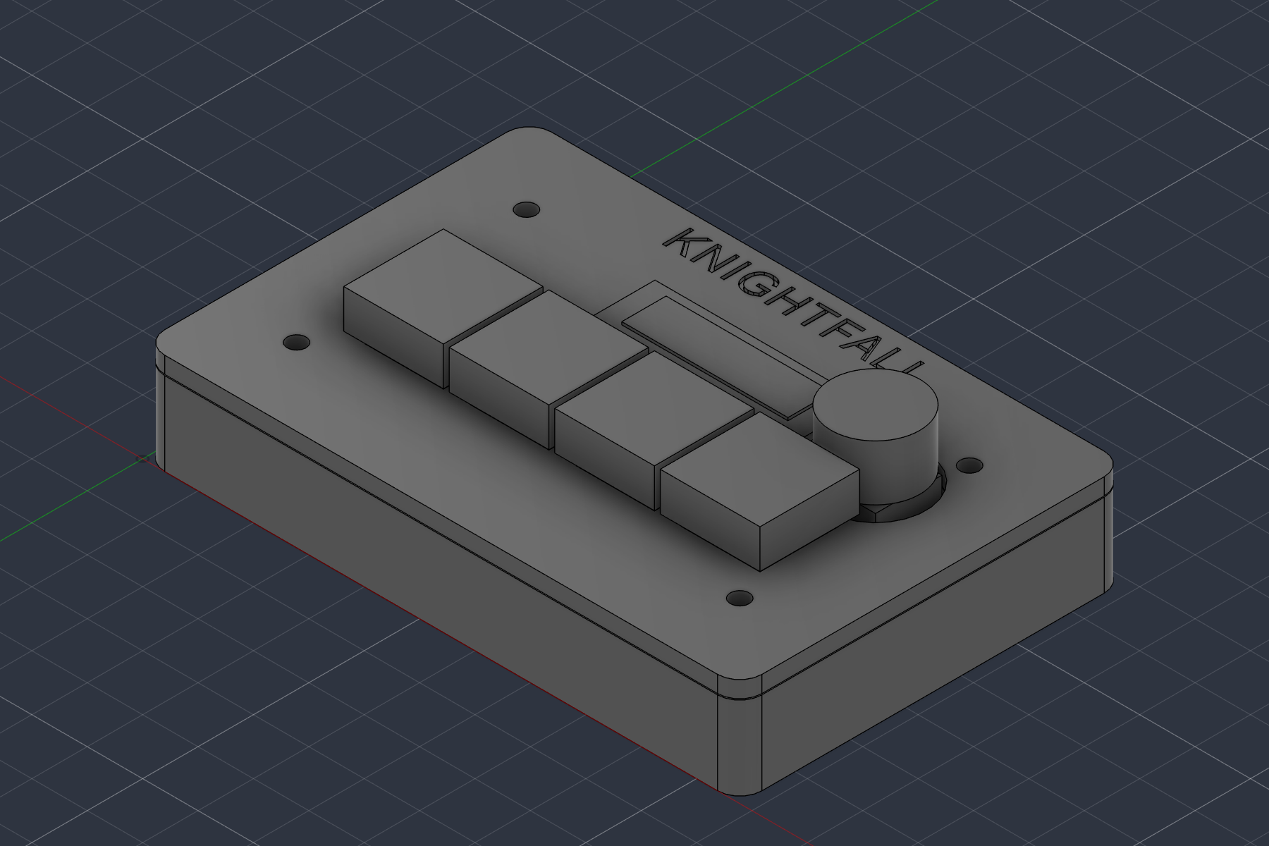
Electronic models are simplified size references, not manufacturer CAD or proof of fit. The case and PCB outline/mounting holes represent the design.
Control - Default action
Four keys, left to right - F13, F14, F15, F16
Press knob - F17
Turn knob - Volume down or up
Assign these keys in the game's or app's settings. VIA can change the keys and knob actions without telling you; four manually selected layers are available. Apps that do not accept F13–F17 can use a different assignment. Check the firmware instructions.
cad/          Complete assembled STEP
pcb/          KiCad project, schematic, board, and local libraries
firmware/     QMK source, VIA definition, build script and report
production/   Gerber ZIP, separate case parts, compiled firmware
assets/       Images, editable Fusion archives, validation reports
README.md
Open Knightfall.kicad_pro in KiCad 10. Custom symbols and footprints are included. The complete assembly includes both case parts and the PCB with mounting holes. Editable Fusion archives are in assets/source.
Vector schematic. Four switches and the encoder push use individual GPIO inputs, so matrix diodes are not needed. The controller mounts underneath the PCB.
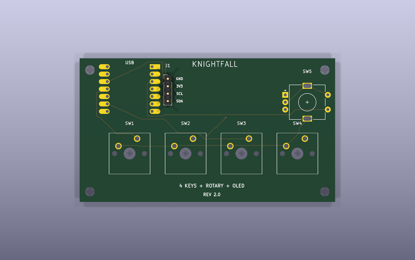
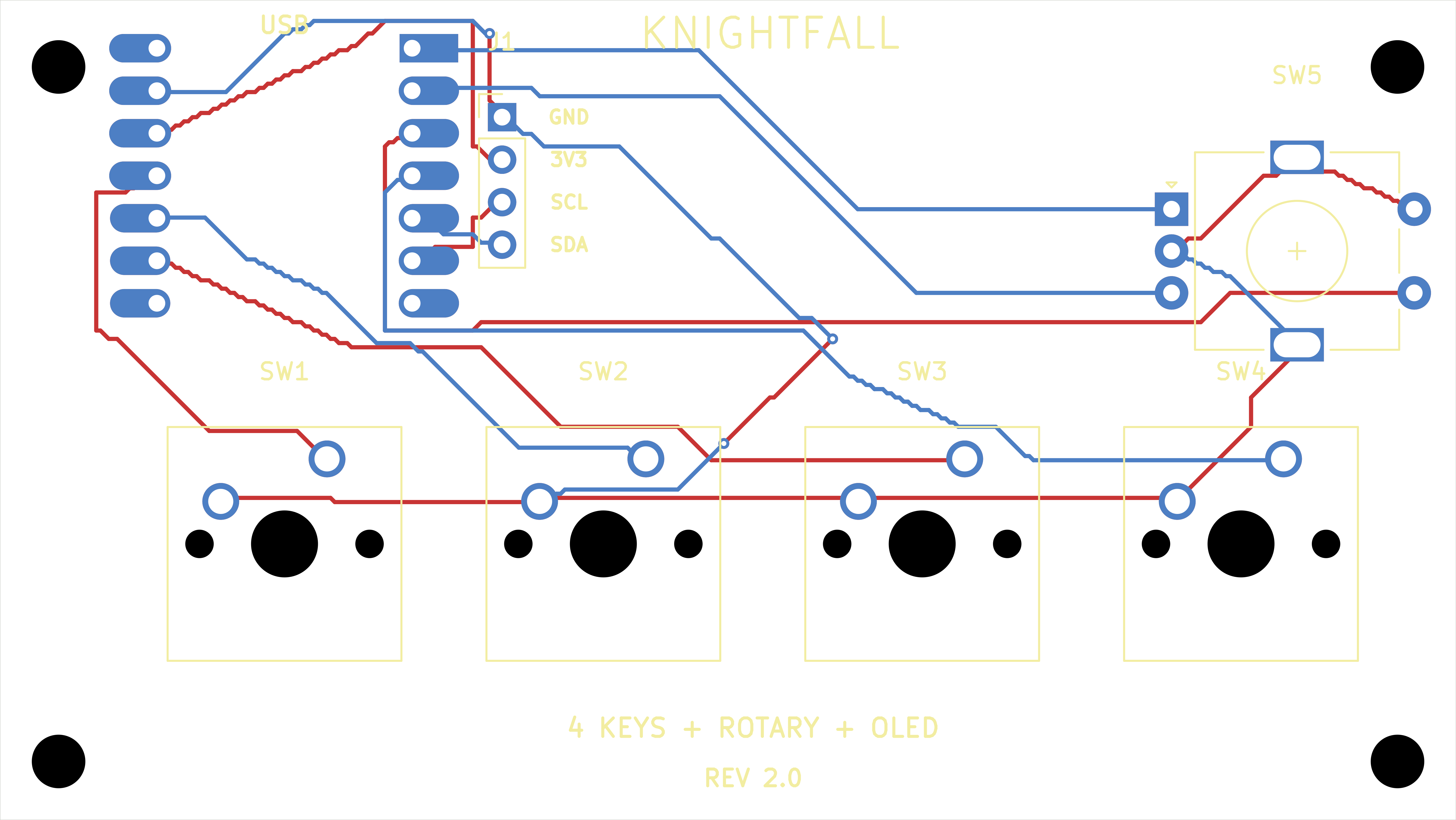
The PCB is 87 × 49 mm, two layers, with a nominal thickness of 1.6 mm. Vector routing view
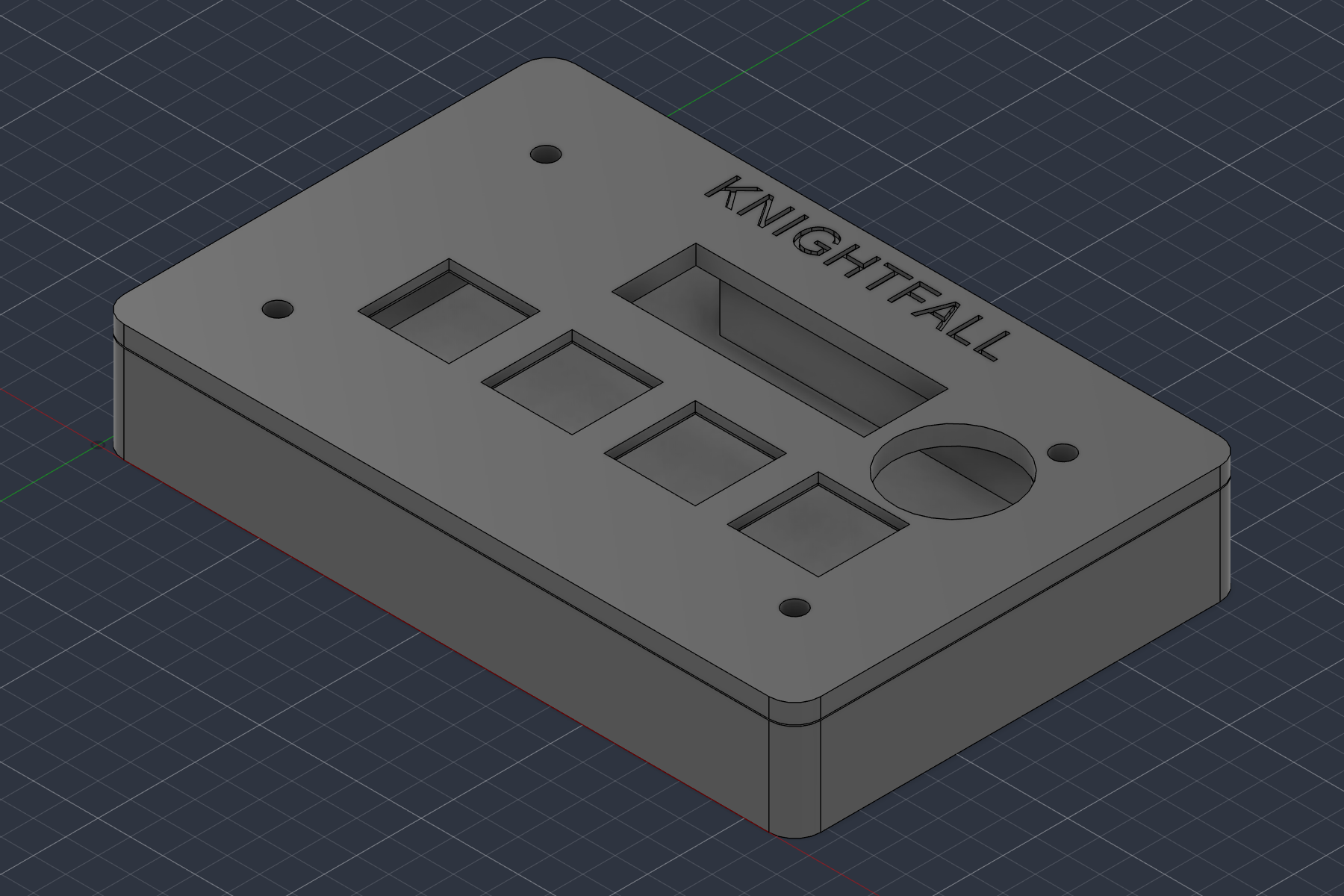
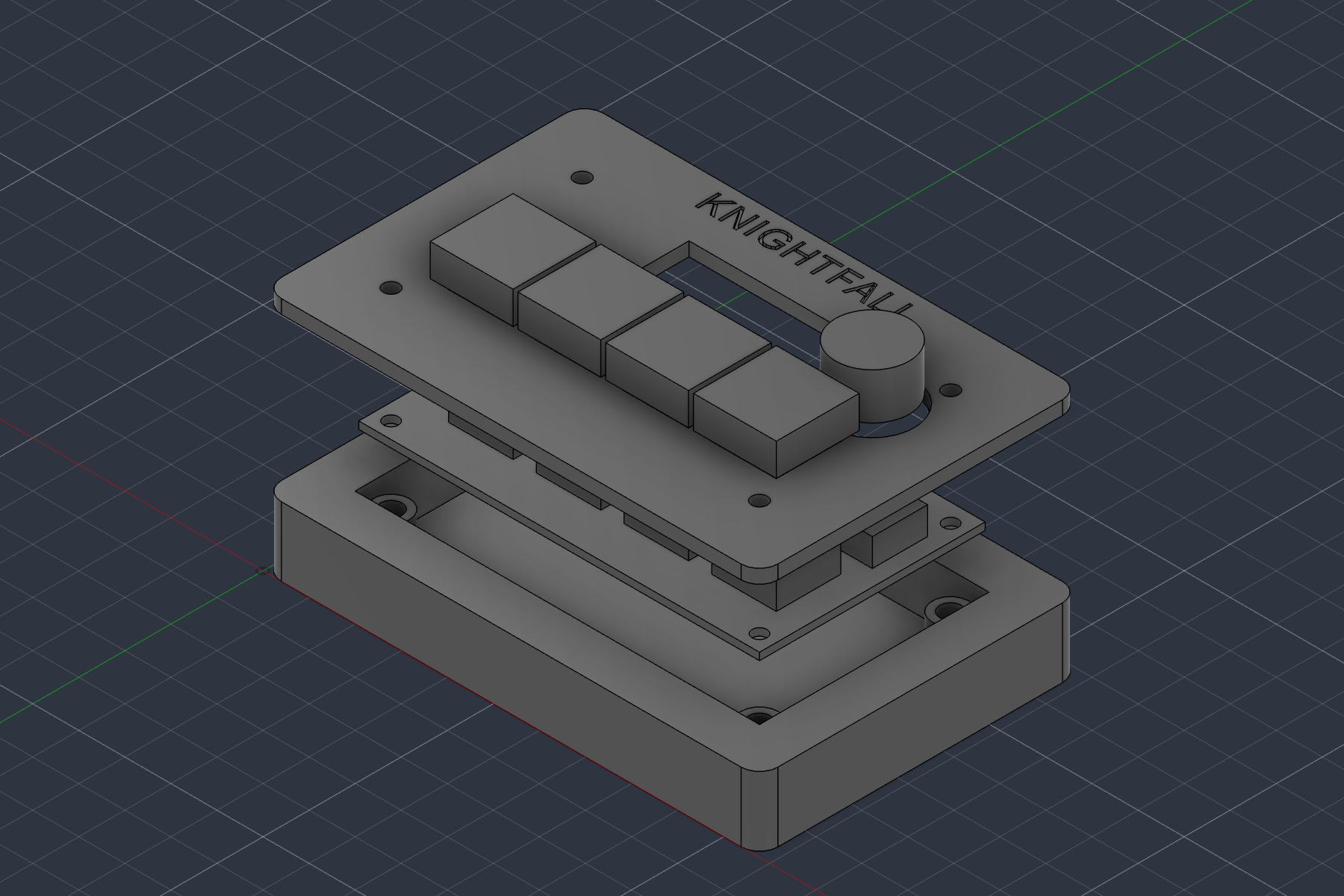
The case is 107.8 × 69.8 × 18.2 mm. Its 87.8 × 49.8 mm cavity leaves 0.4 mm clearance at each PCB edge. Switch openings are 14.1 mm with a 1.5 mm clip lip. Four M3 screws and heat-set inserts secure the assembly.
The exploded view separates the plate, PCB/electronics, and bottom. Dry-fit the actual switches, encoder, OLED, controller, and USB cable before soldering.
No LEDs or diodes are used.
| File | Purpose |
|---|---|
| gerbers.zip | Copper, mask, silk, outline, and plated/non-plated drills |
| Bottom STL | Print one bottom, in millimetres |
| Plate STL | Print one plate, in millimetres |
| Bottom STEP, Plate STEP | Alternate solid exports of those same print parts |
| firmware.uf2 | Compiled QMK VIA firmware for XIAO RP2040 |
Print one of each case part, using either STL or STEP. The complete assembly STEP is a design reference, not a single printable part. Flash the UF2 after obtaining the controller; installation and remapping instructions are included.
QMK and VIA. Firmware retains its license notices. Hardware references include Hackpad resources and the KiCad care package; upstream assets retain their original terms.
| Qty | Value | Footprint | References |
|---|---|---|---|
| 4 | MountingHole | Knightfall:MountingHole_3.2mm_M3 | H1, H2, H3, H4 |
| 4 | SW_Push | Knightfall:SW_Cherry_MX_1.00u_PCB | SW1, SW2, SW3, SW4 |
| 1 | EC11 encoder + push | Knightfall:RotaryEncoder_Alps_EC11E-Switch_Vertical_H20mm | SW5 |
| 1 | OLED GND-VCC-SCL-SDA | Knightfall:PinHeader_1x04_P2.54mm_Vertical | J1 |
| 1 | XIAO_RP2040 | Knightfall:XIAO-Generic-Hybrid-14P-2.54-21X17.8MM | U1 |
It measures 87 × 49 mm and has 2 copper layers, 1.6 mm thick.
11 parts. The full list of its parts is on this page, with links to each part's symbol and footprint where PCBKit's library has them.
From the Seyinlash/Knightfall repository on GitHub, at the commit this page was made from: the board is pcb/Knightfall.kicad_pcb and its schematic pcb/Knightfall.kicad_sch. PCBKit opens the board in the browser, with nothing to install.
Its repository states no licence, so its author keeps all rights: ask Seyinlash before reusing the design.
google/mozc-devices
Circuit diagrams and firmware source code for Gboard DIY keyboards


FrameworkComputer/ExpansionCards
Reference designs and documentation to create Expansion Cards for the Framework Laptop

hoglet67/RGBtoHDMI
Bare-metal Raspberry Pi project that provides pixel-perfect sampling of Retro Computer RGB/YUV video and conversion to HDMI

hackclub/OnBoard
💡 Join 1,000 teenagers and make your first PCB with a $100 grant!


tardate/LittleArduinoProjects
a collection of "Little Electronic & Arduino Projects", most involving electronics or an Arduino in one way or another!

basilfx/TRADFRI-Hacking
Hacking IKEA TRÅDFRI products, such as light bulbs, window blinds and other accessories.