4 layers45 × 19 mm

 sebastiansebs/Arduino-Nano-from-Scratch
Custom-designed microcontroller development board based on the ATmega328P-M. The board integrates a USB-to-serial converter for programming and UART/SPI communication with comprehensive pin headers for flexible interfacing.
Arduino Nano is an open-source printed circuit board by sebastiansebs, from the sebastiansebs/Arduino-Nano-from-Scratch repository on GitHub. It is a 4-layer board of 44 × 18.4 mm with 39 parts on 55 nets, routed with 622 tracks and 48 vias.
It is built around the ATMEGA328P-MU, FT232RL and LM1117MP-5.0. Its parts include 10 capacitors, 7 resistors, 5 diodes, 5 connectors and 3 ICs. It belongs with the interfaces and adapters and microcontroller boards boards and the AVR (ATmega, ATtiny) boards of this library.


This project describes a custom-designed microcontroller development board, similar to an Arduino Nano, based on the ATmega328P-M. The board integrates a stable 5V power supply, a USB-to-serial converter for programming and UART/SPI communication, and comprehensive pin headers for flexible interfacing.
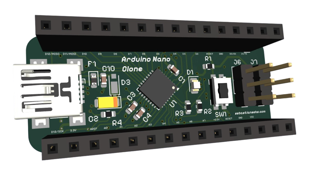
Figure 1: Front view of the PCB
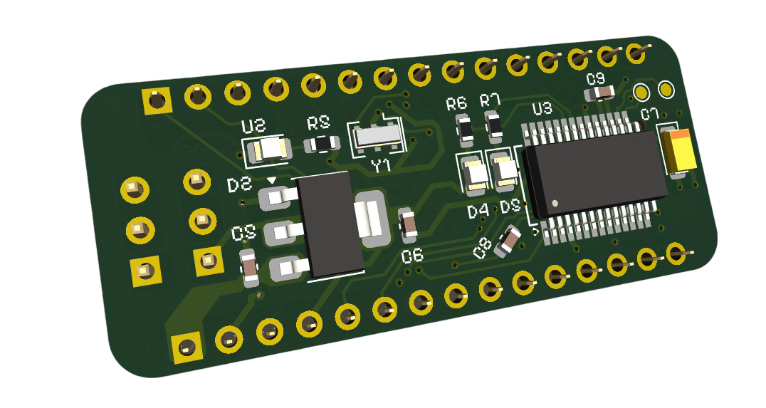
Figure 2: Back view of the PCB
The project is structured hierarchically within KiCad, with the following key sub-schematics:
The PCB is meticulously designed with the following 4 layers to optimize signal integrity, power delivery networks (PDN), and component density, ensuring robust performance and manufacturability:
Layer Top (F.Cu - Front Copper):
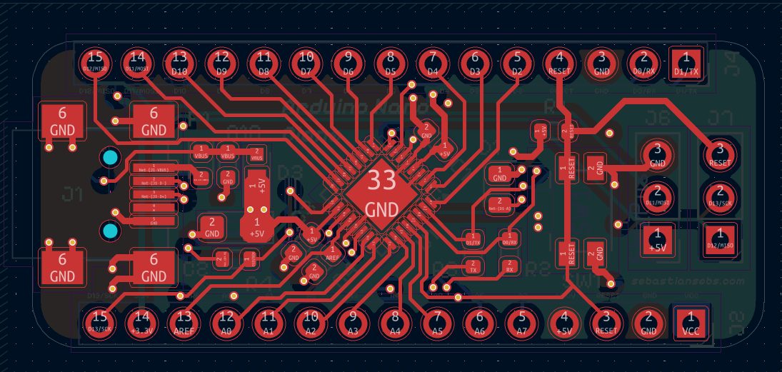
5V (In1.Cu - Inner Copper 1):
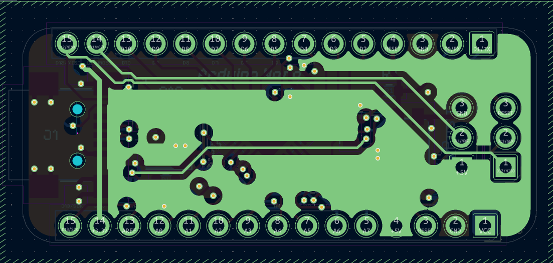
GND (In2.Cu - Inner Copper 2):
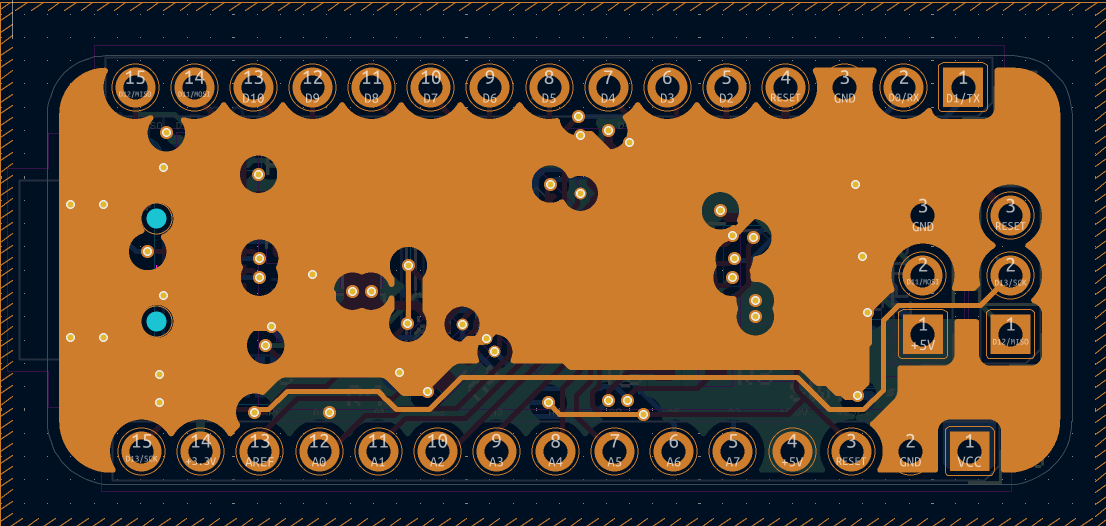
Layer Bottom (B.Cu - Bottom Copper):
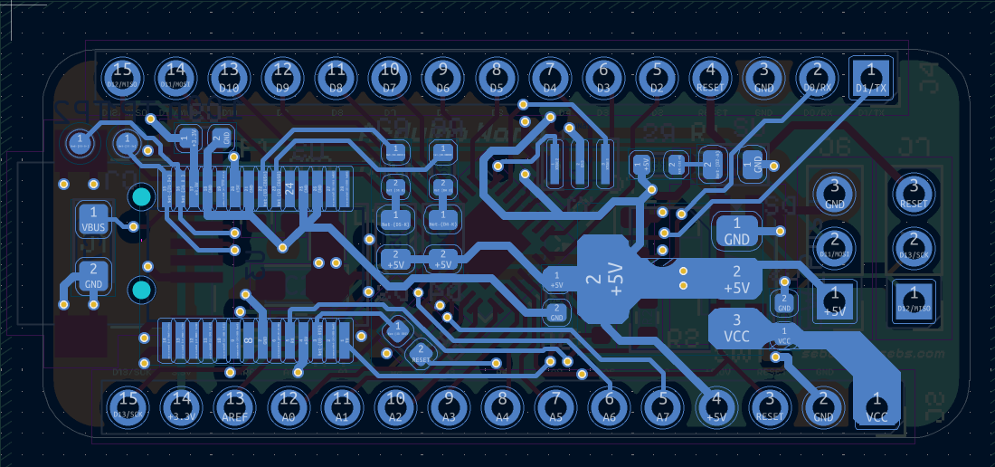
Arduino Nano.kicad_pro: KiCad project file.Arduino Nano.kicad_sch: Top-level schematic.Microcontroller.kicad_sch, Pins.kicad_sch, Power Supply.kicad_sch, USB Port.kicad_sch: Hierarchical sub-schematic files.Arduino Nano.kicad_pcb: PCB layout file.Arduino Nano.kicad_dru: PCB design rules file.Arduino Nano.kicad_prl: Project-specific library settings.| Qty | Value | Footprint | References |
|---|---|---|---|
| 7 | 1k | Resistor_SMD:R_0603_1608Metric | R1, R2, R3, R4, R5, R6, R7 |
| 4 | 1.6mm | MountingHole:MountingHole_2mm | H1, H2, H3, H4 |
| 4 | 100n | Capacitor_SMD:C_0603_1608Metric | C4, C8, C9, C10 |
| 4 | 1u | Capacitor_SMD:C_0603_1608Metric | C1, C3, C5, C6 |
| 2 | 4u7_16V | Capacitor_Tantalum_SMD:CP_EIA-3216-10_Kemet-I | C2, C7 |
| 2 | Conn_01x03_Pin | Connector_PinHeader_2.54mm:PinHeader_1x03_P2.54mm_Vertical | J6, J7 |
| 2 | Conn_01x15_Pin | Connector_PinSocket_2.54mm:PinSocket_1x15_P2.54mm_Vertical | J2, J4 |
| 2 | Green | LED_SMD:LED_0805_2012Metric | D2, D5 |
| 2 | TestPoint_Small | TestPoint:TestPoint_Pad_D1.0mm | TP1, TP2 |
| 1 | 0603 | Diode_SMD:D_0603_1608Metric | F1 |
| 1 | 16MHz | Crystal:Resonator_SMD_Murata_CSTxExxV-3Pin_3.0x1.1mm | Y1 |
| 1 | ATmega328P-M | Package_DFN_QFN:QFN-32-1EP_5x5mm_P0.5mm_EP3.1x3.1mm | U1 |
| 1 | Diode | Diode_SMD:D_MicroSMP_AK | D3 |
| 1 | FT232RL | Package_SO:SSOP-28_5.3x10.2mm_P0.65mm | U3 |
| 1 | LM1117MP-5.0 | Package_TO_SOT_SMD:SOT-223-3_TabPin2 | U2 |
| 1 | Red | LED_SMD:LED_0805_2012Metric | D4 |
| 1 | SW_Push | Button_Switch_SMD:Panasonic_EVQPUK_EVQPUB | SW1 |
| 1 | USB_B_Mini | Connector_USB:USB_Mini-B_Wuerth_65100516121_Horizontal | J1 |
| 1 | Yellow | LED_SMD:LED_0805_2012Metric | D1 |

Hirusha785/arduino-nano-kicad-design
⚙️ Arduino Nano-compatible development board designed in KiCad for the Mastering KiCad Specialization final project. Includes schematic, PCB layout, 3D renders, BOM, and fabrication-ready files for manufacturing. 🚀📐

Rehmanchaudhary/custom-pcb-design
Custom Arduino Nano–compatible board — full schematic and PCB design in KiCad, physically etched and soldered


It measures 44 × 18.4 mm and has 4 copper layers, 1.33 mm thick.
39 parts, built around the ATMEGA328P-MU, FT232RL and LM1117MP-5.0. The full list of its parts is on this page, with links to each part's symbol and footprint where PCBKit's library has them.
From the sebastiansebs/Arduino-Nano-from-Scratch repository on GitHub, at the commit this page was made from: the board is Arduino-Nano/Arduino Nano.kicad_pcb and its schematic Arduino-Nano/Arduino Nano.kicad_sch. PCBKit opens the board in the browser, with nothing to install.
Its repository states no licence, so its author keeps all rights: ask sebastiansebs before reusing the design.