
2 layers10.7 × 10 mm
SBK PFET1
sbarabe/SBK_FET1
Logic-level N-channel and P-channel MOSFET modules for education, breadboarding, and prototyping.
4 partsCERN-OHL-P-2.0

 sbarabe/SBK_FET1
Logic-level N-channel and P-channel MOSFET modules for education, breadboarding, and prototyping.
SBK NFET1 is an open-source printed circuit board by sbarabe, from the sbarabe/SBK_FET1 repository on GitHub, published under the CERN-OHL-P-2.0 licence. It is a 2-layer board of 10.7 × 10 mm with 4 parts on 5 nets, routed with 4 tracks and 4 vias.
It is built around the AO3400A. Its parts include 1 resistor, 1 diode, 1 transistor and 1 connector. It belongs with the interfaces and adapters and microcontroller boards boards of this library.
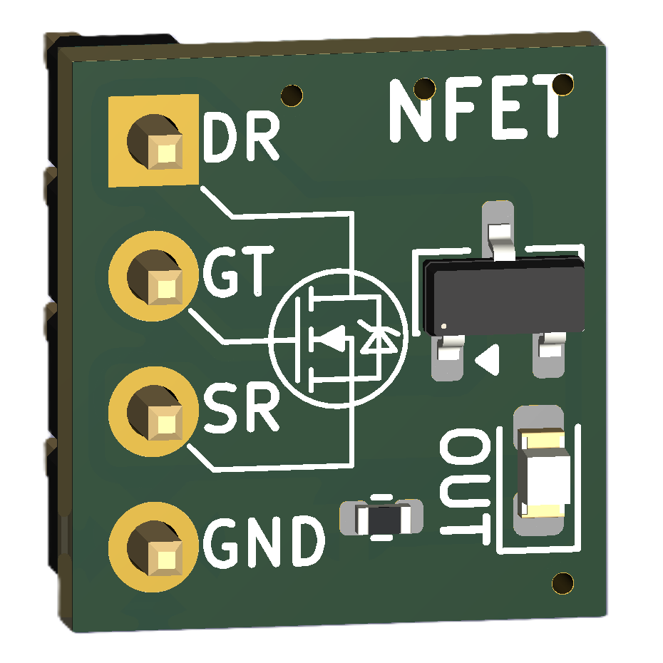
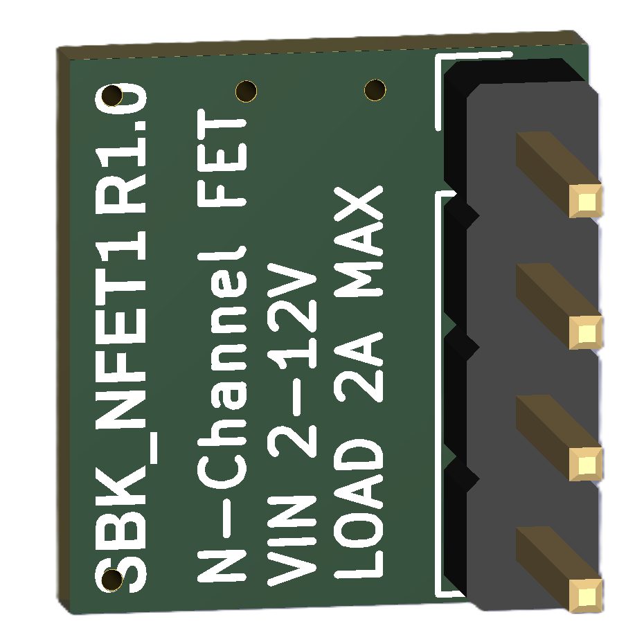
NFET Front NFET Back
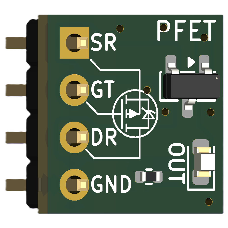
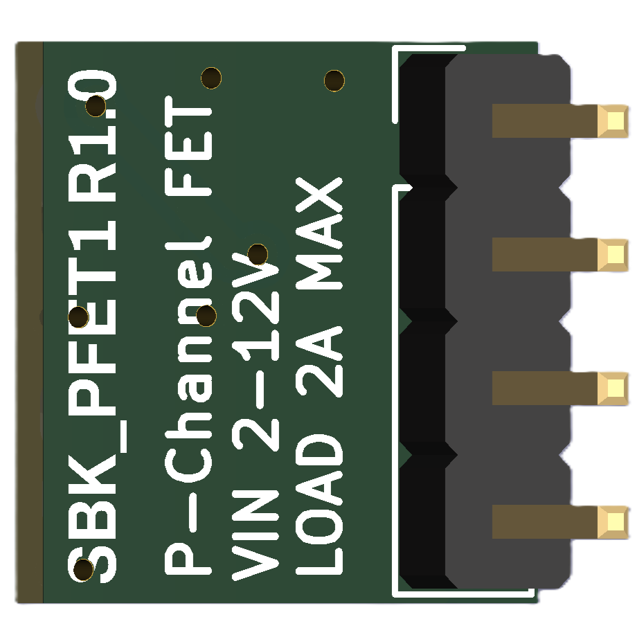
PFET Front PFET Back
SBK_FET1 is a compact educational MOSFET module designed for breadboards, prototyping, and learning electronic switching circuits.
The module is available in both N-channel and P-channel versions and provides clearly labeled Drain, Gate, and Source connections. An optional output voltage indicator LED can be enabled by connecting the GND pin or disabled by leaving it unconnected.
| Pin | Description |
|---|---|
| DR | Drain |
| GT | Gate |
| SR | Source (OUT) |
| GND | Optional ground connection for the OUT status indicator LED |
| Pin | Description |
|---|---|
| SR | Source |
| GT | Gate |
| DR | Drain (OUT) |
| GND | Optional ground connection for OUT status indicator LED |
Note: The GND pin is only required to power the status indicator LED. The MOSFET operates normally without it.
The status indicator LED monitors the OUT terminal. On SBK_NFET1, OUT is the Source terminal. On SBK_PFET1, OUT is the Drain terminal.
This project is fully open-source hardware. You can:
If you would prefer fully assembled modules rather than assembling the PCBs yourself, I can provide professionally assembled modules in small batches on demand.
For availability, pricing, or custom quantities, please contact:
Assembled modules are intended for hobbyists, educators, prototypes, and small-scale projects. Availability depends on component stock and production capacity.
Suggestions, bug reports, and improvements are welcome.
To report a problem or suggest an improvement, open an Issue. Pull Requests are also welcome for corrections, documentation improvements, and design changes that make the project easier to understand or build.
If this project is useful for learning, teaching, or prototyping, you can support its continued development.
Donations help fund prototype hardware, documentation, educational resources, and future open-source projects.
❤️ Support the project through PayPal
Thank you for supporting open-source educational hardware.
This project is released as open-source hardware under the CERN Open Hardware Licence Version 2 - Permissive (CERN-OHL-P v2).
You are free to study, modify, manufacture, and distribute this design under the terms of the license.
See the LICENSE file for details.
Designed using KiCad 10.
| Qty | Value | Footprint | References |
|---|---|---|---|
| 1 | 1 x 3 pin header | Connector_PinHeader_2.54mm:PinHeader_1x04_P2.54mm_Vertical | J1 |
| 1 | 15 kΩ | Resistor_SMD:R_0402_1005Metric | R2 |
| 1 | AO3400A | Package_TO_SOT_SMD:SOT-23 | Q1 |
| 1 | RED | LED_SMD:LED_0603_1608Metric | D1 |
sbarabe/SBK_FET1
Logic-level N-channel and P-channel MOSFET modules for education, breadboarding, and prototyping.


brickbots/PiFinder
A plate solving telescope finder based around a Raspberry PI and RPI HQ Camera


MickiusMousius/Rolio46Keyboard
A split wireless keyboard based on the Corne and Sofle
It measures 10.7 × 10 mm and has 2 copper layers, 1.6 mm thick.
4 parts, built around the AO3400A. The full list of its parts is on this page, with links to each part's symbol and footprint where PCBKit's library has them.
From the sbarabe/SBK_FET1 repository on GitHub, at the commit this page was made from: the board is SBK_NFET1/KiCad/SBK_NFET1.kicad_pcb and its schematic SBK_NFET1/KiCad/SBK_NFET1.kicad_sch. PCBKit opens the board in the browser, with nothing to install.
Its repository publishes it under the CERN-OHL-P-2.0 licence: you may reuse it on that licence's terms (keep the author's notice, and for a copyleft licence share your changes alike).