4 layers185 × 90 mm
Coil driver
enemonsieur/TIMS_analyses
Analyses of TIMS stimulation + EEG for Characterization.
52 parts

 samanbeer/PCB_Ruler
Why: - Is is cool, the schooll is coming :O and i dont have a ruler :)
Ruler kicad is an open-source printed circuit board by samanbeer, from the samanbeer/PCB_Ruler repository on GitHub. It is a 2-layer board of 304.9 × 35 mm with 18 parts on 58 nets, routed with 68 tracks and 0 vias.
It is built around the 2EDL23N06PJXUMA1 and 74LVC1G11GW. Its parts include 11 resistors, 4 capacitors and 3 ICs.


https://FORGE.hackclub.com/projects/1713
Why:

Schematic is randomly connected so it looks good on PCB (not supposed to work :D):
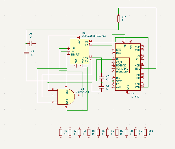
This is a Ruler made as PCB in KiCAD and InkScape(for .svg editing).
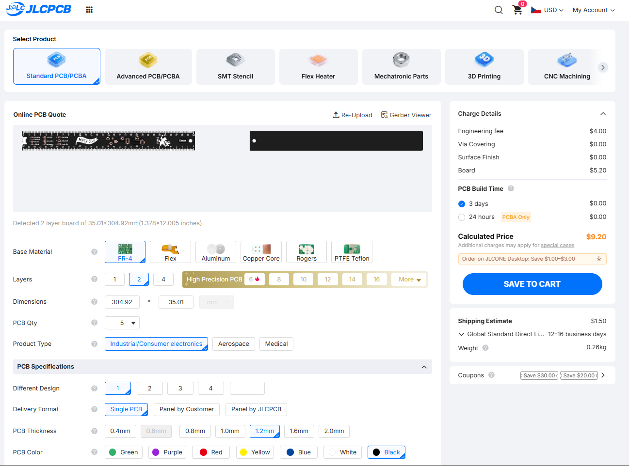
Here is JLCPCB cart:
Rendered Image:

| What | PRICE |
|---|---|
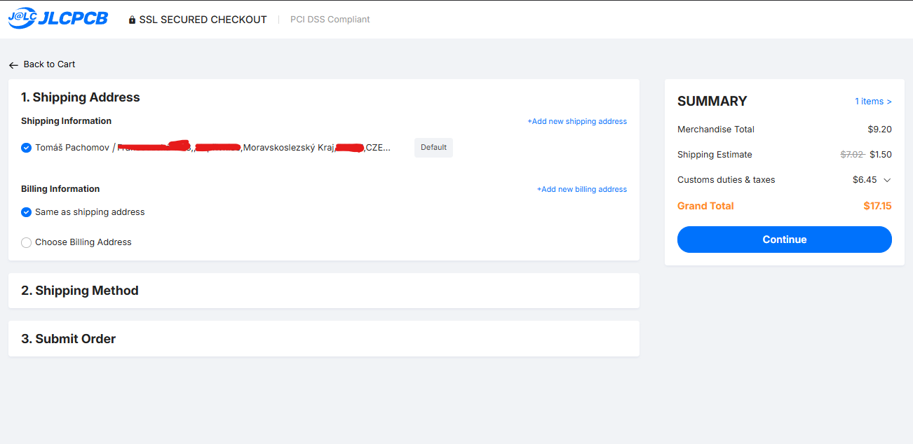
| PCB (Ruler) + shipping + Customs | 17.15 USD |
note: I dont need components since I will not solder them on the ruler. The components footprints are for design
Detailed photos:
[Image blocked: detailed1]
[Image blocked: detailed2]
The precision is great, at the end it has offest just by 0.5mm which is great
[Image blocked: precision]
| Qty | Value | Footprint | References |
|---|---|---|---|
| 2 | C | Capacitor_SMD:C_1812_4532Metric_Pad1.57x3.40mm_HandSolder | C2, C3 |
| 2 | R | Resistor_SMD:R_2010_5025Metric | R10, R11 |
| 1 | 2EDL23N06PJXUMA1 | Package_SO:SOIC-14_3.9x8.7mm_P1.27mm | U1 |
| 1 | 74LVC1G11 | Package_TO_SOT_SMD:SOT-223-6 | U3 |
| 1 | C | Capacitor_SMD:C_Elec_5x5.4 | C1 |
| 1 | C | Capacitor_SMD:C_0805_2012Metric | C4 |
| 1 | R | Resistor_SMD:R_0612_1632Metric | R3 |
| 1 | R | Resistor_SMD:R_1210_3225Metric | R8 |
| 1 | R | Resistor_SMD:R_1206_3216Metric | R7 |
| 1 | R | Resistor_SMD:R_0508_1220Metric | R1 |
| 1 | R | Resistor_SMD:R_1812_4532Metric | R9 |
| 1 | R | Resistor_SMD:R_0603_1608Metric | R2 |
| 1 | R | Resistor_SMD:R_0805_2012Metric | R4 |
| 1 | R | Resistor_SMD:R_1020_2550Metric | R6 |
| 1 | R | Resistor_SMD:R_0815_2038Metric | R5 |
| 1 | iC-HTG | Package_DFN_QFN:HVQFN-24-1EP_4x4mm_P0.5mm_EP2.5x2.5mm | U2 |
enemonsieur/TIMS_analyses
Analyses of TIMS stimulation + EEG for Characterization.


Popax21/framework16-cellular
A M.2 cellular modem Expansion Bay module for the Framework Laptop 16

macnetic/rp2040-cubesat
A CubeSat Onboard Computer, using the RP2040 microcontroller.


Hob-dev/Pockey
A play on the word "Pocket", this keyboard is meant to be ultra-portable ultra-low profile using Cherry ULP, with a magnetic enclosure mechanism that let's you fit the keyboard in your pocket.


ajisrawi/sentinel-uhf-radar
Reference design of a two-face UHF early-warning phased-array radar: system sizing, MoM antenna simulation, seven KiCad PCB projects, Blender site model
It measures 304.9 × 35 mm and has 2 copper layers, 1.6 mm thick.
18 parts, built around the 2EDL23N06PJXUMA1 and 74LVC1G11GW. The full list of its parts is on this page, with links to each part's symbol and footprint where PCBKit's library has them.
From the samanbeer/PCB_Ruler repository on GitHub, at the commit this page was made from: the board is ruler_kicad.kicad_pcb and its schematic ruler_kicad.kicad_sch. PCBKit opens the board in the browser, with nothing to install.
Its repository states no licence, so its author keeps all rights: ask samanbeer before reusing the design.