4 layers97.6 × 74.8 mm
Project byte hamr
robertrico/project_byte_hamr
Open source expansion platform for Apple IIe prototyping and development
93 parts2

 robertrico/project_byte_hamr2
Open source expansion platform for Apple IIe prototyping and development
Byte ravn is an open-source printed circuit board by robertrico, from the robertrico/project_byte_hamr repository on GitHub. It is a 4-layer board of 109.5 × 74.8 mm with 36 parts on 108 nets, routed with 607 tracks and 64 vias.
It is built around the TLV62569DBVR-TP, SN74LVC8T245PW and CX0603MRX7R8BB223, with the CC0805ZKY5V5BB226, RT0603FRE073K3L and STPS2L30AF among its other parts. Its parts include 12 capacitors, 7 ICs, 7 connectors, 1 diode and 1 inductor.


An open-source FPGA expansion card for the Apple II family of computers.
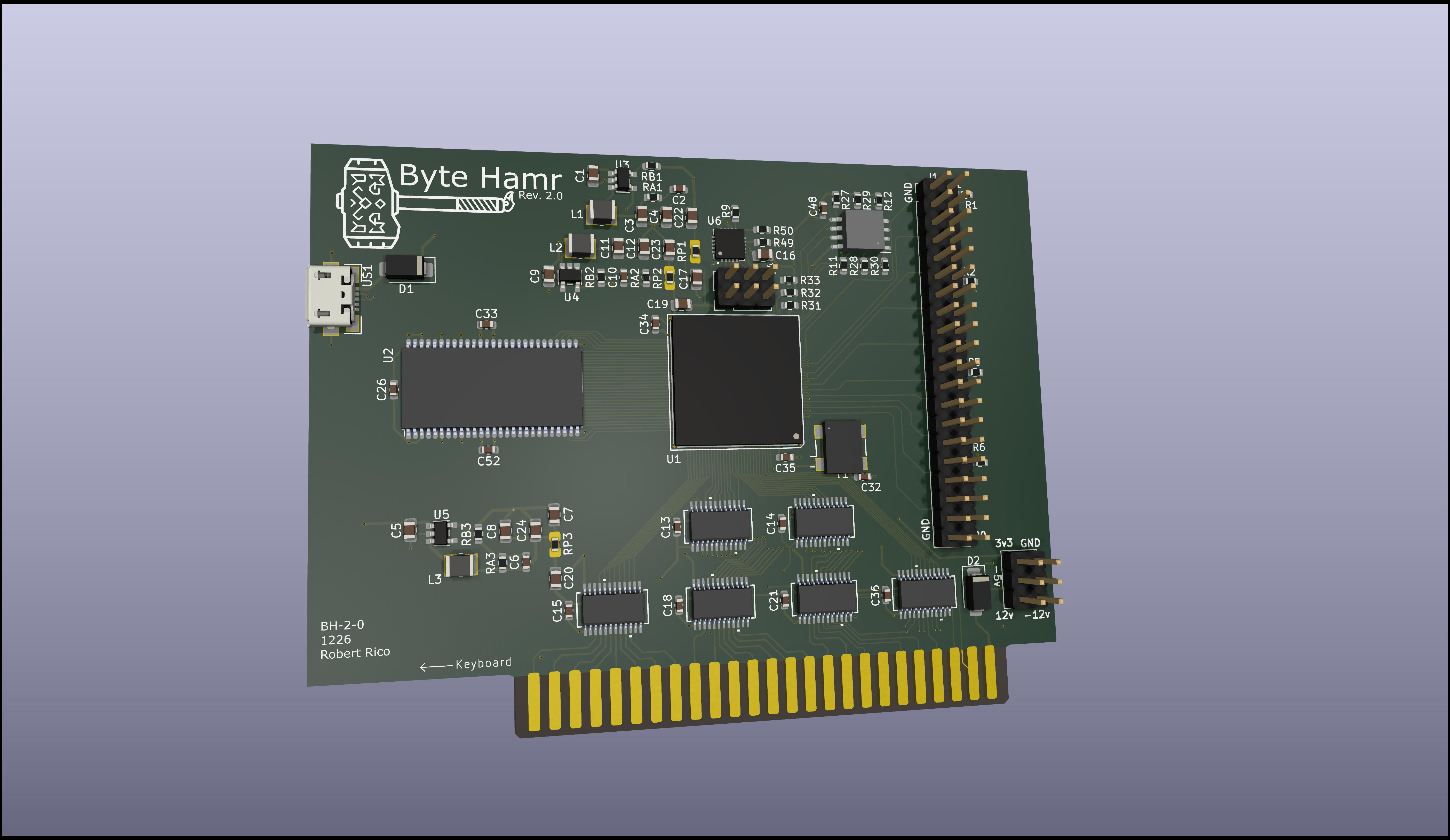
Byte Hamr brings modern FPGA capabilities to the Apple II, II+, IIe, and IIgs. Unlike purpose-built cards that serve a single function, Byte Hamr is a general-purpose platform for developing and running custom hardware designs on vintage Apple hardware.
The card sits between the simplicity of the A2FPGA (which targets HDMI output) and the complexity of the Carte Blanche (which is difficult to obtain and uses proprietary tooling). Byte Hamr uses the Lattice ECP5 FPGA with full support for the open-source Yosys/nextpnr toolchain.
| Parameter | Value |
|---|---|
| FPGA | Lattice ECP5-85F (LFE5U-85F-8BG381I) |
| Logic Elements | 84K LUTs |
| Block RAM | 3744 Kbit |
| SDRAM | 64MB, 16-bit bus |
| Flash | 128Mb SPI |
| USB | Full-speed via FT231XQ |
| GPIO | 20 pins, 3.3V LVCMOS33 |
| Oscillator | 100 MHz (Rev 2) |
| Power | +5V from USB or Apple II slot |
| Dimensions | Standard Apple II card form factor |
                                    +------------------+
                                    |     SDRAM        |
                                    |   (64MB x16)     |
                                    +--------+---------+
                                             |
+-------------+     +----------+     +-------+--------+     +----------+
| Apple II    |     | Level    |     |                |     |   SPI    |
| Expansion   +---->+ Shifters +---->+   ECP5-85F     +---->+  Flash   |
| Slot        |     | (5V/3.3V)|     |     FPGA       |     |  (16MB)  |
+-------------+     +----------+     +-------+--------+     +----------+
                                             |
                                     +-------+--------+
                                     |      USB       |
                                     |  (FT231XQ)     |
+----------------+Three on-board switching regulators generate the required voltages:
Power can be sourced from USB (+5V) or the Apple II slot, with Schottky diode OR-ing for automatic switching. Rev 2 moves the 5V input diode ahead of the level-shifter rail so USB alone can power the bus logic.
Six 74LVC8T245 bidirectional level shifters translate between the Apple II's 5V bus and the FPGA's 3.3V I/O. The interface provides access to:
Rev 2 adds a dedicated 74AHC1G04 inverter (U7) that generates the correct-polarity DIR control for the data-bus transceiver, and exposes the transceiver's OE on an FPGA pin so gateware can cleanly gate drive.
20-pin header with ground interleaving (pin 1 marked at the top, 20 at the bottom). All pins are 3.3V LVCMOS33.
| GPIO | FPGA Site | GPIO | FPGA Site | |
|---|---|---|---|---|
| GPIO_1 | P3 | GPIO_11 | J1 | |
| GPIO_2 | P1 | GPIO_12 | H2 | |
| GPIO_3 | P2 | GPIO_13 | H1 | |
| GPIO_4 | N1 | GPIO_14 | G2 | |
| GPIO_5 | M1 | GPIO_15 | G1 | |
| GPIO_6 | L2 | GPIO_16 | F2 | |
| GPIO_7 | L1 | GPIO_17 | F1 | |
| GPIO_8 | K3 | GPIO_18 | E2 | |
| GPIO_9 | K1 | GPIO_19 | E1 | |
| GPIO_10 | K2 | GPIO_20 | D2 |
See byte_hamr.lpf for full pin constraints.
Rev 2 — fabricated and bring-up in progress (April 2026). Both boards enumerate over USB and pass initial SDRAM + GPIO tests.
Rev 1 — sent to fabrication (December 2025). Tagged rev1 in git; all Rev 1 gateware preserved under gateware/rev1/.
See VERSION.md for full version history.
DATA_OE, B20)nRES_READ input (A5) so gateware can monitor Apple II resetproject_byte_hamr/
├── hardware/
│ └── byte_hamr/ # Main FPGA card
│ ├── kicad/ # KiCad schematic and PCB
│ ├── bom/ # Bill of materials
│ └── gerbers/ # Manufacturing files
├── gateware/
│ ├── rev1/ # Rev 1 designs (frozen, matches rev1 git tag)
│ │ ├── constraints/
│ │ ├── signal_check/
│ │ ├── sdram_test/
│ │ ├── sdram_bank/
│ │ ├── pattern_rom/
│ │ ├── logic_hamr/
│ │ ├── smart_hamr/
│ │ ├── block_hamr/
│ │ └── flash_hamr/
│ └── rev2/ # Rev 2 designs (porting in progress)
│ ├── constraints/
│ └── signal_check/
├── software/
│ ├── ASM/ # 6502 assembly source (Merlin32)
│ ├── LOGICHAMR/ # Logic analyzer disk contents
│ └── utils/ # Disk image utilities
└── docs/ # DocumentationGateware:
6502 Assembly:
Disk Utilities:
Builds are selected by DESIGN and REV. REV defaults to rev1; set REV=rev2 when targeting the current hardware.
make                                # Build default (REV=rev1, DESIGN=signal_check)
make DESIGN=xxx                     # Build specific design (rev1)
make DESIGN=xxx REV=rev2            # Build against Rev 2 pinout
make sim DESIGN=xxx REV=rev2        # Run simulation
make wave                           # Run simulation and open GTKWave
make help                           # Show all available targets
b8008_hamr lives under gateware/rev2/ and always needs REV=rev2; it also
needs fusesoc installed and a sibling intel-8008-vhdl checkout
(INTEL8008_DIR, default ~/Development/intel-8008-vhdl) to generate its
netlist at build time, e.g. make DESIGN=b8008_hamr REV=rev2 bit.
make DESIGN=xxx REV=rev2 prog                         # Program via JTAG (volatile)
make DESIGN=xxx REV=rev2 prog-flash                   # Program SPI flash (persistent)
make DESIGN=xxx REV=rev2 prog-flash SERIAL=<FTDI_SN> # Target a specific board┌─────────────┐ ┌───────────────┐ ┌─────────────┐ ┌───────────┐
│ Merlin32 │────▶│ AppleCommander│────▶│ ADTPro │────▶│ Apple IIe │
│ (assemble) │ │ (create .dsk) │ │ (transfer) │ │ (run) │
└─────────────┘ └───────────────┘ └─────────────┘ └───────────┘# 1. Edit source in software/LOGICHAMR/*.S
# 2. Assemble with Merlin32
make assemble ASM_SRC=software/LOGICHAMR/LOGIC.S
# 3. Create disk image (auto-copied to ADTPro disks folder)
make create-dsk DSK=LOGICHAMR
# 4. Transfer via ADTPro to real hardware
# 5. On Apple II: BRUN LOGICDisk utilities:
make extract-dsk DSK=file.dsk     # Extract files from disk image
make list-dsk # List disks in ADTPro foldermake pinout # Regenerate FPGA pinout from schematics
make lpf # Regenerate LPF constraints
make clean # Remove build filesRev 1 versions (proven on Rev 1 hardware):
| Design | Description |
|---|---|
| signal_check | Board bring-up test (SDRAM, GPIO, bus monitor) |
| sdram_test | Register-driven SDRAM access from Apple II |
| sdram_bank | SDRAM bank-switching controller |
| pattern_rom | SDRAM-backed pattern ROM for display testing |
| logic_hamr | 8-channel logic analyzer with HIRES display |
| smart_hamr | SmartPort/IWM disk controller with ESP32 companion |
| block_hamr | ProDOS block device with SDRAM and SPI flash persistence |
| flash_hamr | SD card ProDOS block device (PicoRV32 + FatFS) |
Rev 2 port: signal_check ported and validated; other designs pending.
Bringup sequence for new boards:
GPIO_9..GPIO_20C0C0:01 → C0C0, then 02, 04, … 80This project builds on the work of others:
"Hamr" is Old Norse for "shape" or "form" — the concept of shapeshifting in Norse mythology. Byte Hamr: shapeshifting bytes. An FPGA that can become any hardware you define. The shape changes based on what you program it to be.
This project is released under the MIT License.
Robert Rico
This is an early-stage project. Issues, suggestions, and pull requests welcome.
| Qty | Value | Footprint | References |
|---|---|---|---|
| 6 | 22nF | Capacitor_SMD:C_0603_1608Metric | C13, C14, C15, C18, C21, C36 |
| 6 | SN74LVC8T245 | footprints:DBQ24-L | U8, U9, U11, U12, U13, U14 |
| 4 | MountingHole_Pad | MountingHole:MountingHole_3mm_Pad | H1, H2, H3, H4 |
| 3 | 22uF | Capacitor_SMD:C_0805_2012Metric | C5, C7, C8 |
| 2 | 2.2uF | Capacitor_SMD:C_0805_2012Metric | C20, C24 |
| 1 | 0 | jumper:R_0805_2012Metric_Pad1.29x1.40mm_HandSolder_Jumper_NC | RP3 |
| 1 | 100pF | Capacitor_SMD:C_0603_1608Metric | C6 |
| 1 | 15k | Resistor_SMD:R_0603_1608Metric | RA3 |
| 1 | 2.2uH | L_1008_1210:L_1008_1210 | L3 |
| 1 | 3.3k | Resistor_SMD:R_0603_1608Metric | RB3 |
| 1 | Bus_Apple_II_Card_Side | PCM_MA_Connector_AppleII:Peripheral_Bus_Edge | J3 |
| 1 | Conn_01x04_Socket | Connector_PinHeader_2.54mm:PinHeader_1x04_P2.54mm_Horizontal | J5 |
| 1 | Conn_01x05_Socket | Connector_PinHeader_2.54mm:PinHeader_1x05_P2.54mm_Horizontal | J6 |
| 1 | Conn_01x07_Socket | Connector_PinHeader_2.54mm:PinHeader_1x07_P2.54mm_Horizontal | J7 |
| 1 | Conn_01x08_Socket | Connector_PinHeader_2.54mm:PinHeader_1x08_P2.54mm_Horizontal | J4 |
| 1 | Conn_01x09_Socket | Connector_PinHeader_2.54mm:PinHeader_1x09_P2.54mm_Horizontal | J2 |
| 1 | Conn_01x16_Socket | Connector_PinHeader_2.54mm:PinHeader_1x16_P2.54mm_Horizontal | J1 |
| 1 | LOGO | LOGO | G*** |
| 1 | STPS2L40AF | Diode_SMD:D_SMA | D2 |
| 1 | TLV62569DBV | TSOT-25:TSOT-25 | U5 |
robertrico/project_byte_hamr
Open source expansion platform for Apple IIe prototyping and development


hackclub/reflow
A YSWS for the northern hemisphere's summer and the aussie's winter. Run by @pmnlla, with love and loads of carrots.

lsartory/Clavier
An FPGA-based mechanical keyboard with an integrated USB hub and communication interfaces

EnriqueNeyra/aether
All-in-one home air quality monitor measuring Temp, Humidity, CO2, VOCs, Particulate Matter, and NOx. Powered by ESP32-C3 running esphome, and built with Home Assistant integration


jlcjak/astra_piNas
Six-layer CM5 Lite dual-NVMe carrier with PCIe switch, Ethernet, microSD, USB-C PD and PoE. Review design; fabrication hold documented.
It measures 109.5 × 74.8 mm and has 4 copper layers, 1.6 mm thick.
36 parts, built around the TLV62569DBVR-TP, SN74LVC8T245PW, CX0603MRX7R8BB223 and CC0805ZKY5V5BB226. The full list of its parts is on this page, with links to each part's symbol and footprint where PCBKit's library has them.
From the robertrico/project_byte_hamr repository on GitHub, at the commit this page was made from: the board is deprecated/byte_ravn/kicad/byte_ravn.kicad_pcb and its schematic deprecated/byte_ravn/kicad/byte_ravn.kicad_sch. PCBKit opens the board in the browser, with nothing to install.
Its repository states no licence, so its author keeps all rights: ask robertrico before reusing the design.