



6 layers304.8 × 243.8 mm

 raszpl/386RC-162
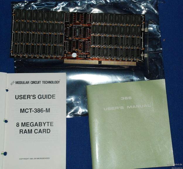
Modular Circuit Technology 386RC-16 ram expansion board for C386-33 reproduction
386RC-16 is an open-source printed circuit board by raszpl, from the raszpl/386RC-16 repository on GitHub, published under the GPL-3.0 licence. It is a 4-layer board of 328.7 × 121.7 mm with 62 parts on 288 nets, routed with 4,112 tracks and 349 vias.
It is built around the 74F240PC and 74F244D. Its parts include 16 ICs, 1 connector and 1 switch.
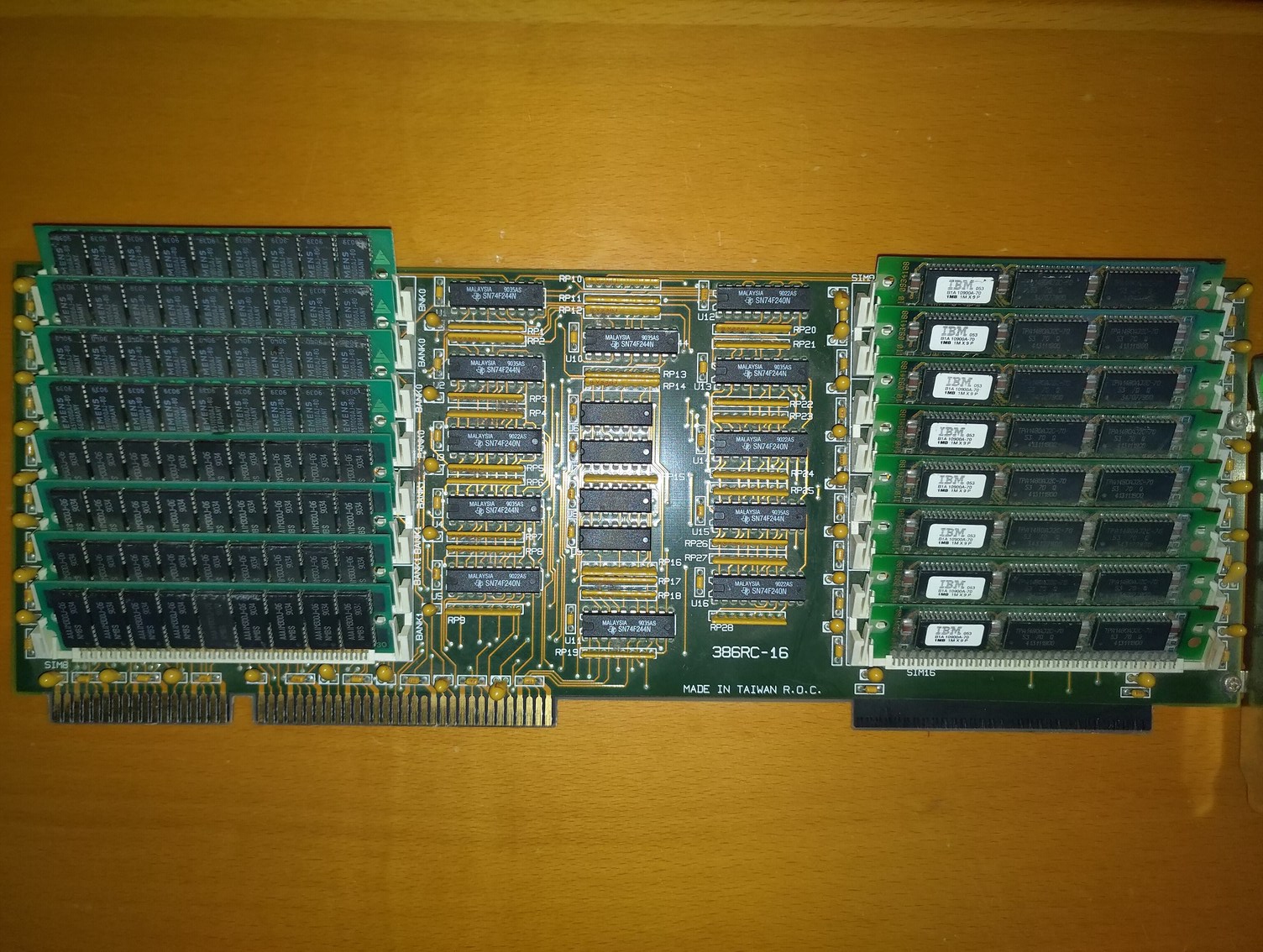
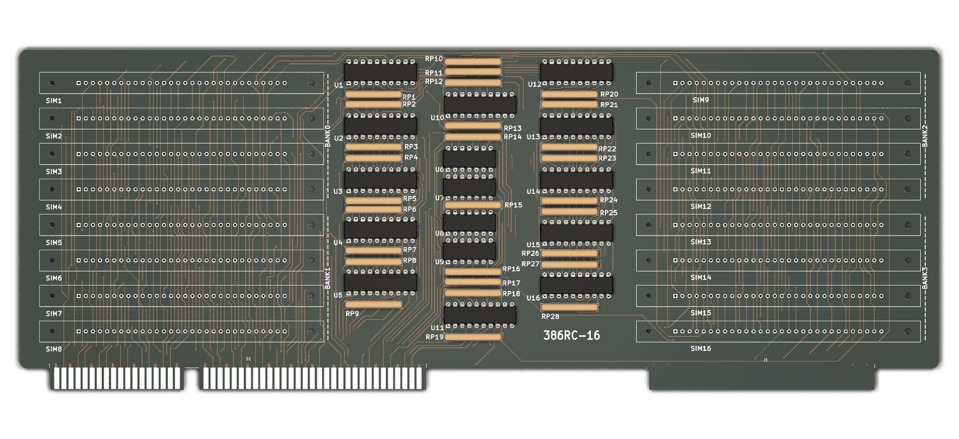
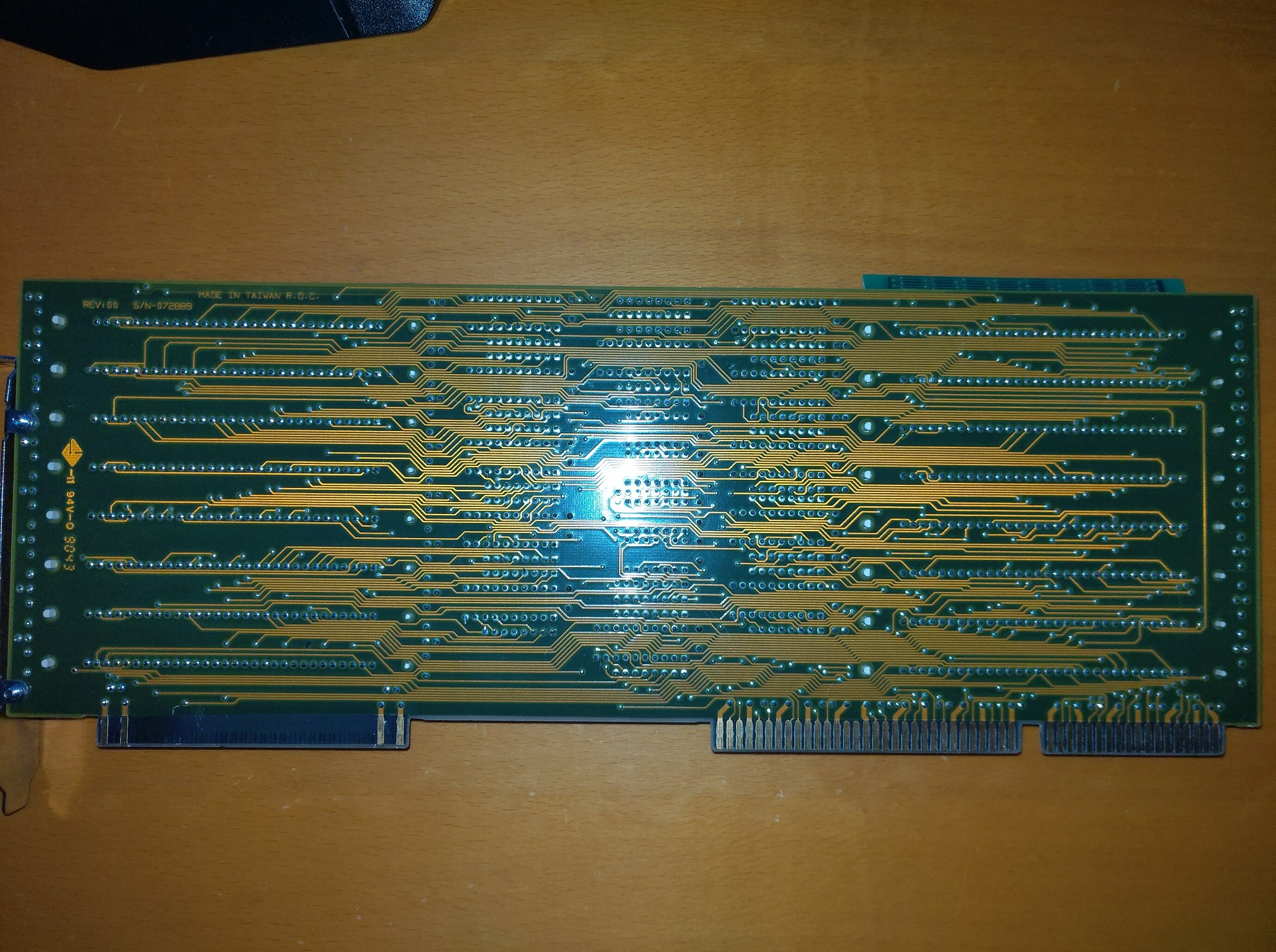
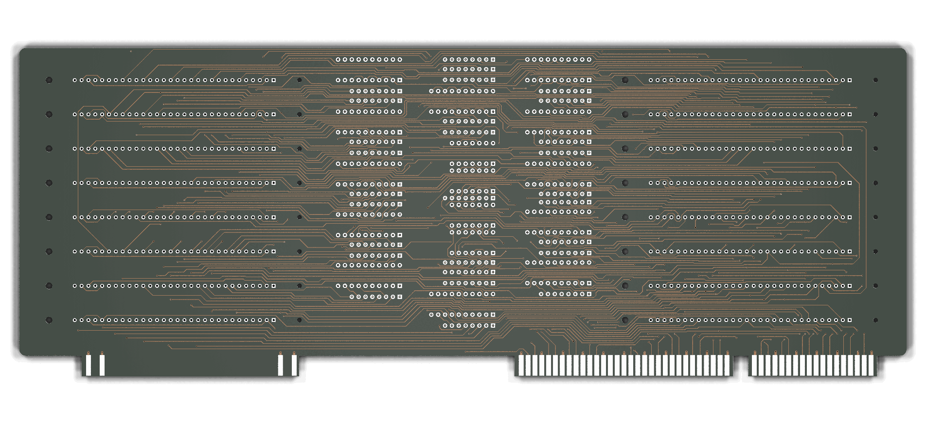
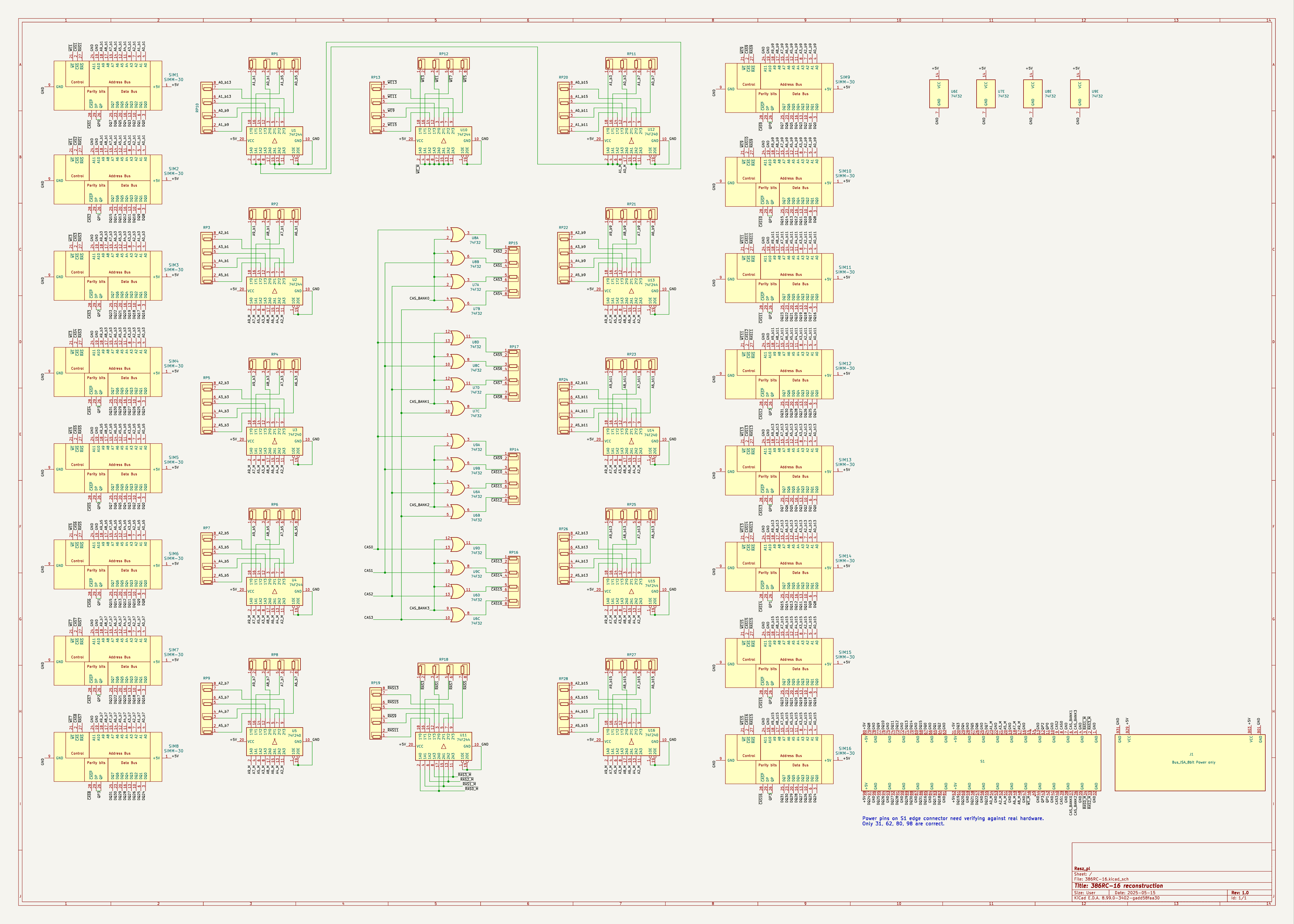
Reverse Engineered non standard ram expansion board for use in Modular Circuit Technology C386-33.
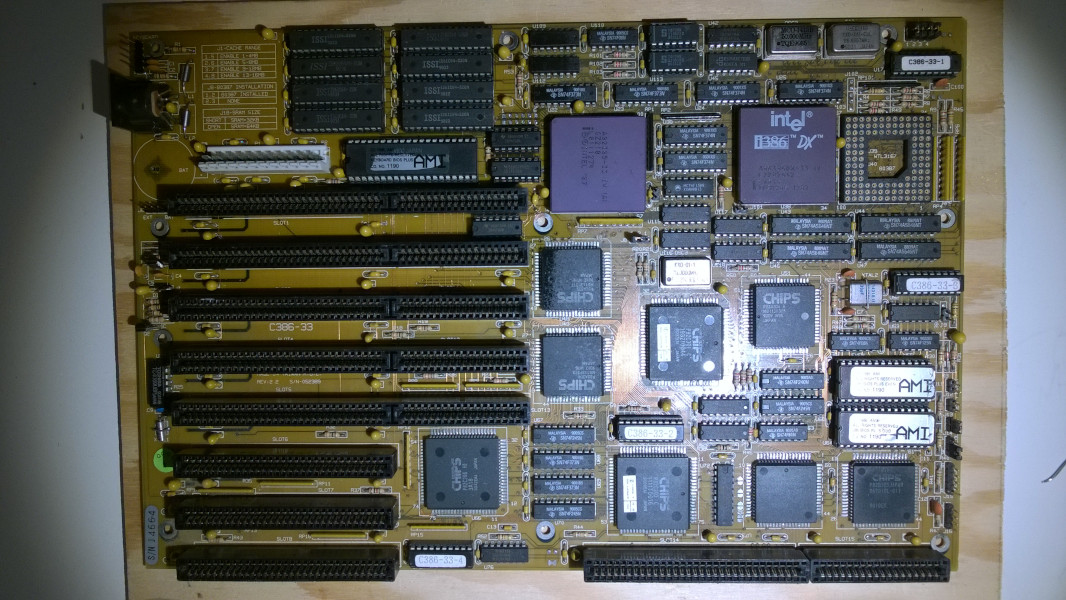
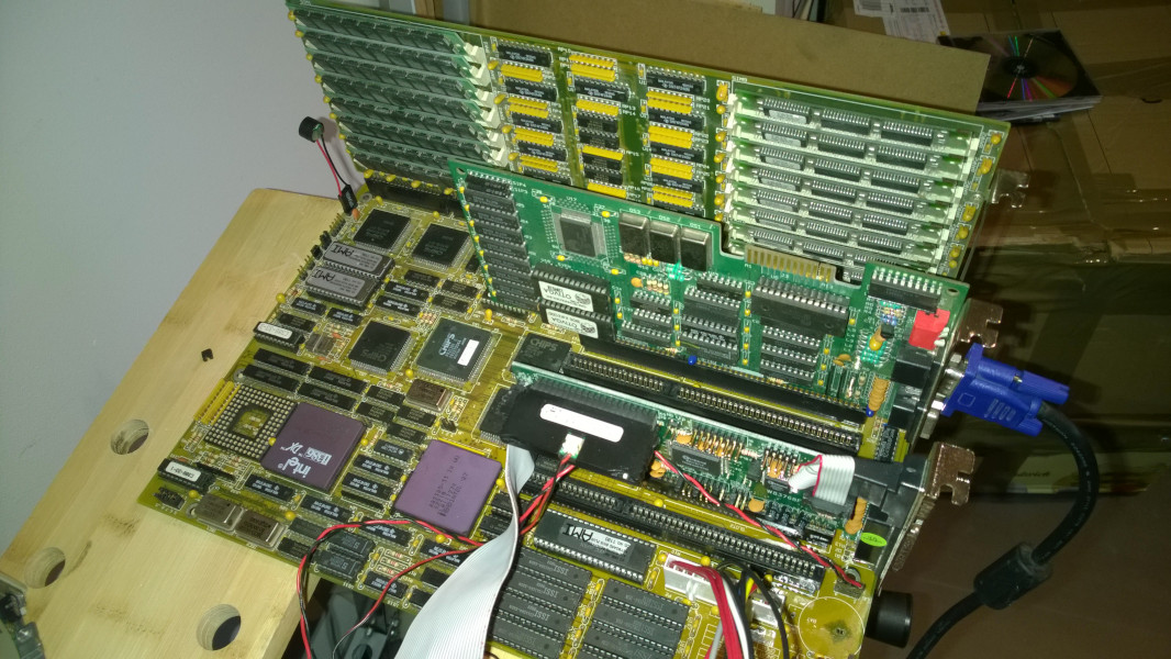
Diagram (png,pdf). Interesting detail about design - it exposes two ways of driving CAS (Column Address Strobe) signals. Designer made it flexible enough to be able to work with different memory controllers/interleave configurations. One set of four CAS pins drives consecutive SIMM sockets in every Bank, the other 4 pin set drives whole banks per CAS line. Brilliant.
Potentially also compatible motherboards:
Incompatible platforms using similar slot. Either wrong offset, orientation or dimensions:
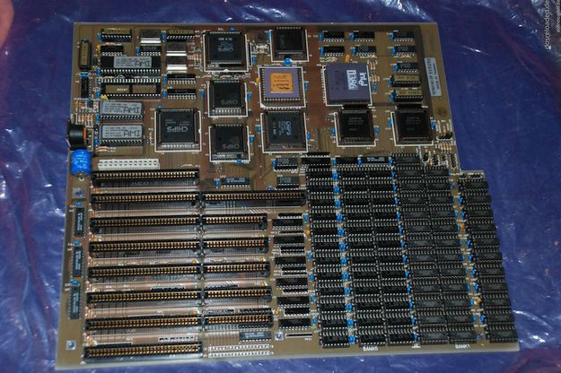
 Grand daddy of C386-33 from 1987, 386DX 20 and IIT FPU 387 20Mhz.
Those six pictures uploaded by McBierle was the only source of information. Provided all vias, back tracks and about 25% front ones. Rest is obscured by components and had to be deduced logically using knowledge of vintage memory subsystems.
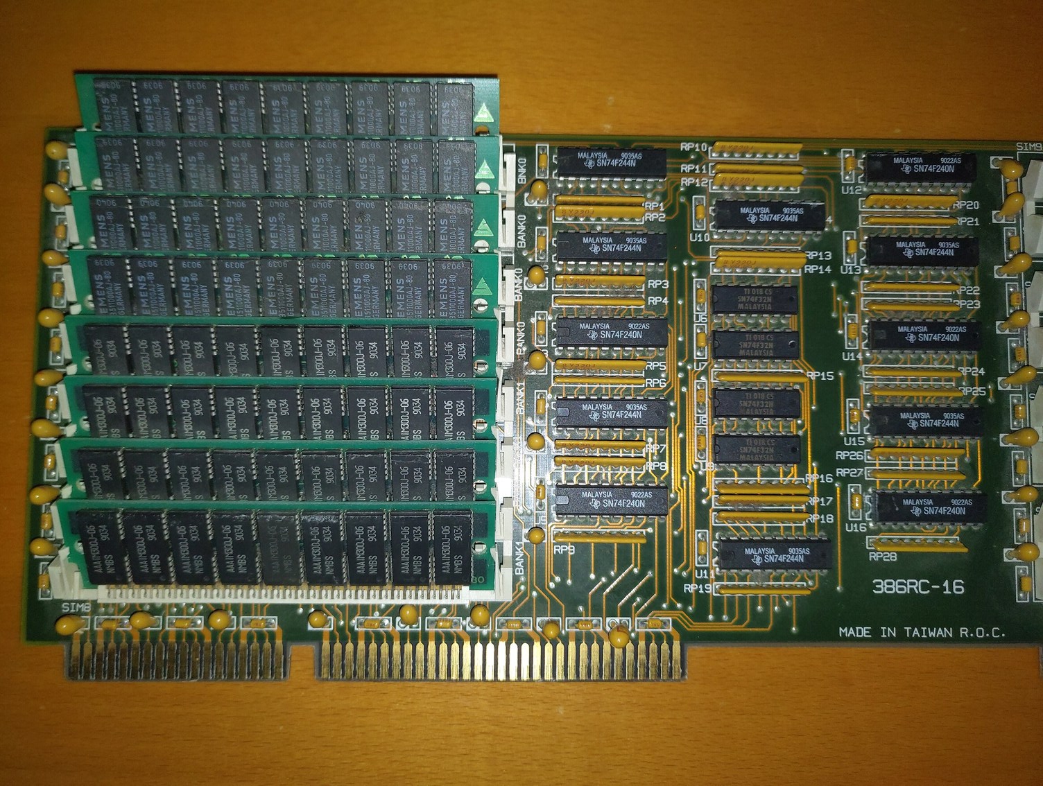
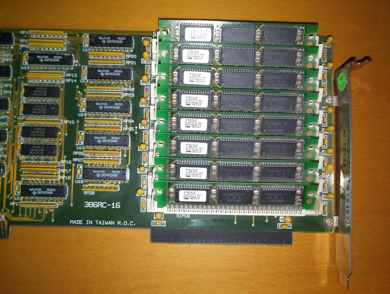
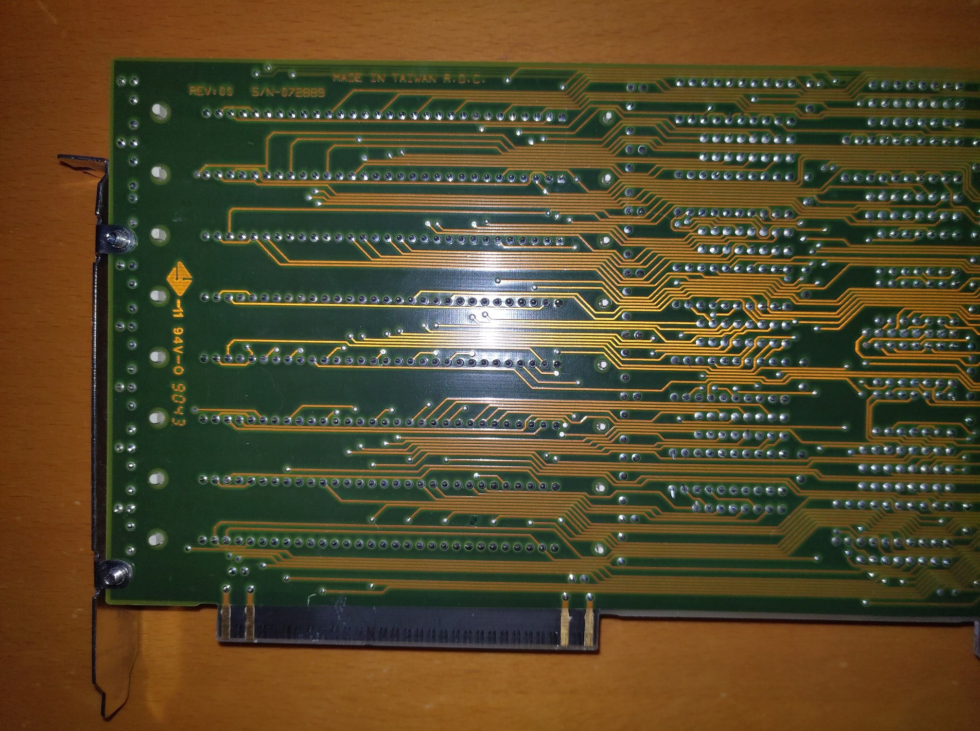
McBierle authored Vogons Story about C386-33 and me thread.
100% reconstructed schematic. 95% ready for manufacturing, remaining tasks:
5/15/2025: Got bored and played with routing. Old board 100% following original track/via layout had track length 3360cm and 381 vias. New optimized layout track length 3341 cm, 349 vias. 20cm shorter tracks and 30 less vias, nice.
11/9/2024: 100% schematic. 100% electrical PCB. Woke up, looked at the CAS mess and immediatelly knew how to route it, magic of a good night's sleep! 0 ERC, 0 DRC errors. 1 DRC warning for unused Via. No idea if original Designer left it unused or somehow routed the board in different way. Personally I dont see a way to use this Via in any way :)
11/8/2024: 95%. SIMM slots and DIP14 chips obscure CAS traces. Struggling hard with routing CAS lines with all the missing information, still dont undertand purpose of OR gates instead of simple buffers
11/7/2024: 85-90% Got RAS mapping correct. 90% back
11/6/2024: 60-80%. Deduced Address/WE buss pairing, Address/Data buss Edge Slot pinout. Still ~300 ERC, ~200 ERC errors.
11/5/2024: 65%. Figured all 240/244 chips used same connections to corresponding pair of Resistor Pair Packs, Designer copy pasted it 12 times.
11/4/2024: 60%. Further fixed picture distortions wih Gimp Transform functionality (what a pain!). Allowed almost ideal component placement and drawing board outline.
10/31/2024: Very VIP. Preliminarily undistorted source pictures using ShiftN to help with more precise component placement. 10% there front10% back
10/30/2024: Project start. Looking at pictures of 386RC-16 uploaded by McBierle on vogons forum and assesing feasibility. Rougly placing components more or less by eye and tracing few lines. 1% there
Interested in having a piece of hardware reverse engineered/cloned? Drop me an email.
| Qty | Value | Footprint | References |
|---|---|---|---|
| 20 | 22 Ohm | Resistor_THT:R_Array_SIP8 | RP1, RP10, RP11, RP12, RP13, RP14, RP15, RP16, RP17, RP18, RP19, RP20, RP21, RP22, RP23, RP24 +4 |
| 16 | SIMM-30 | 386RC-16:SIMM | SIM1, SIM2, SIM3, SIM4, SIM5, SIM6, SIM7, SIM8, SIM9, SIM10, SIM11, SIM12, SIM13, SIM14, SIM15, SIM16 |
| 8 | 22Ohm | Resistor_THT:R_Array_SIP8 | RP2, RP3, RP4, RP5, RP6, RP7, RP8, RP9 |
| 7 | 74F244 | Package_DIP:DIP-20_W7.62mm | U1, U2, U4, U10, U11, U13, U15 |
| 5 | 74F240 | Package_DIP:DIP-20_W7.62mm | U3, U5, U12, U14, U16 |
| 4 | 74F32 | Package_DIP:DIP-14_W7.62mm | U6, U7, U8, U9 |
| 1 | Bus_ISA_16bit | Connector_PCBEdge:BUS_AT | S1 |
| 1 | Bus_ISA_8bit Power only | 386RC-16:ISA Power only | J1 |
It measures 328.7 × 121.7 mm and has 4 copper layers, 1.6 mm thick.
62 parts, built around the 74F240PC and 74F244D. The full list of its parts is on this page, with links to each part's symbol and footprint where PCBKit's library has them.
From the raszpl/386RC-16 repository on GitHub, at the commit this page was made from: the board is 386RC-16.kicad_pcb and its schematic 386RC-16.kicad_sch. PCBKit opens the board in the browser, with nothing to install.
Its repository publishes it under the GPL-3.0 licence: you may reuse it on that licence's terms (keep the author's notice, and for a copyleft licence share your changes alike).


skiselev/micro_8088
Micro 8088 - IBM XT Compatible Processor Board based on Faraday FE2010 chipset

monotech/NuXT
MicroATX Turbo XT Motherboard, with VGA, Floppy, CF, Serial


monotech/Nano8088
Smaller SMD version of Sergey Kiselev's Micro 8088 SBC, with XT-CF added

raymondh2/CompaqPortableIII
Current PCB Memory Expansion board layout is untested. The backplane for the expansion cards is tested and working.