4 layers184.9 × 243.8 mm
Project NuXT
monotech/NuXT
MicroATX Turbo XT Motherboard, with VGA, Floppy, CF, Serial
223 parts121GPL-3.0

 skiselev/micro_8088412
Micro 8088 - IBM XT Compatible Processor Board based on Faraday FE2010 chipset
8088-FE2010A SBC is an open-source printed circuit board by skiselev, from the skiselev/micro_8088 repository on GitHub, published under the GPL-3.0 licence. It is a 2-layer board of 152.4 × 101.6 mm with 72 parts on 178 nets, routed with 3,101 tracks and 139 vias.
It is built around the PIC12F629-I/P, 74F245D and 74F573D, with the 74F244D and PN2222A among its other parts. Its parts include 23 capacitors, 16 ICs, 8 resistors, 3 connectors and 3 switches. It belongs with the computers and single-board computers boards and the FPGA and CPLD and PIC boards of this library.


IBM XT Compatible Processor Board based on Faraday FE2010/FE2010A chipset
Micro 8088 is an easy to build IBM PC/XT compatible processor board. It uses a fairly common Faraday FE2010/FE2010A chipset, that implements most of IBM PC/XT LSIs (Intel 8xxx ICs) and glue logic. Micro 8088 uses SRAM ICs to implement the system RAM, and a Flash ROM IC to store the BIOS, further reducing the number of components, and simplifying the build process.
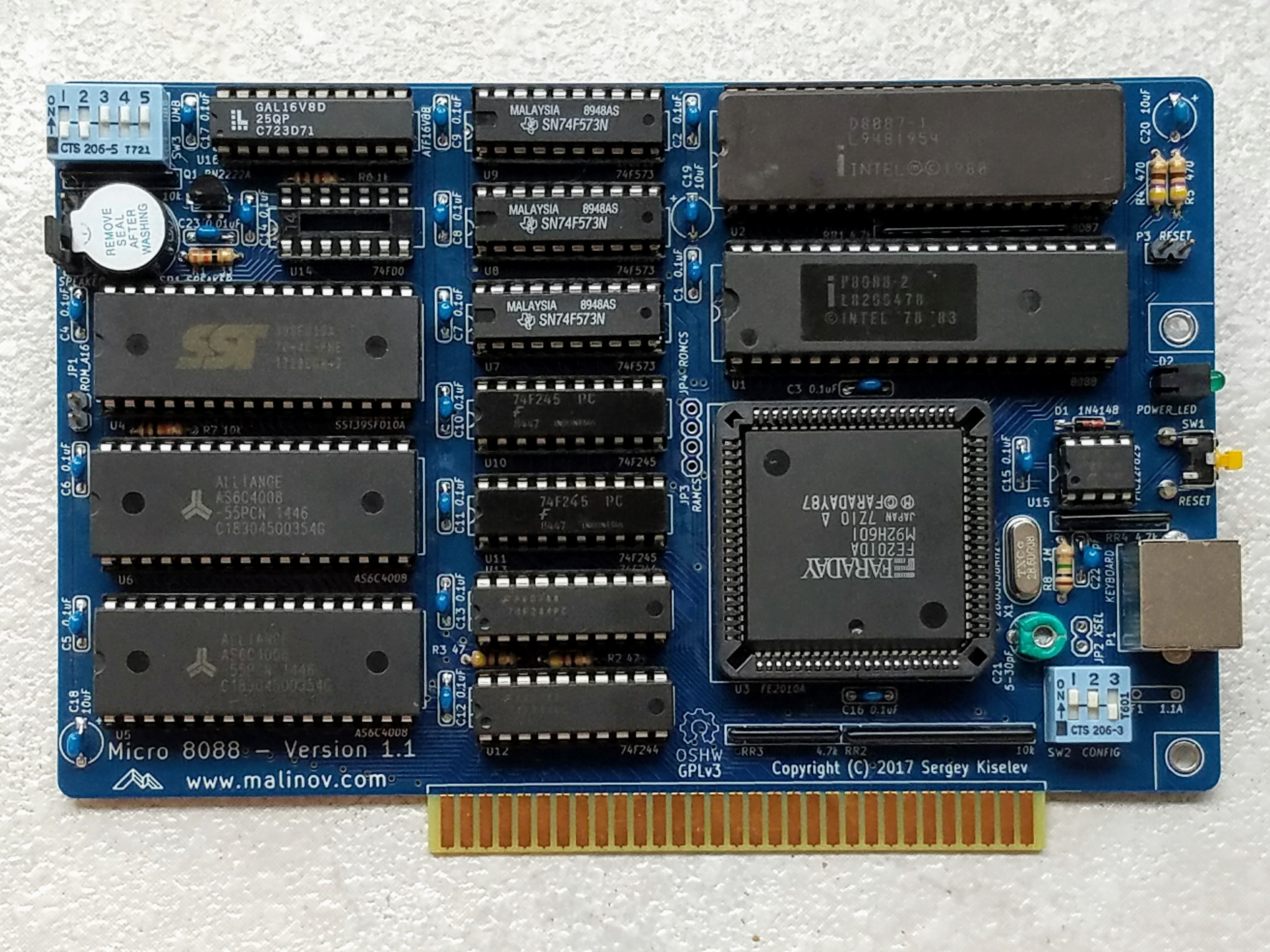
Please refer to Building Instructions page for detailed instructions.
Please refer to Faraday FE2010A documentation and Faraday FE2010 datasheet for detailed information about Faraday FE2010/FE2010A chipsets.
Note: CPU clock frequency switching (turbo mode) is only implemented in Faraday FE2010A chipset (not in FE2010).
| Pin | Description |
|---|---|
| 1 | Keyboard data |
| 2 | Unused |
| 3 | GND |
| 4 | +5V |
| 5 | Keyboard clock |
| 6 | Unused |
| Pin | Description |
|---|---|
| 1 | Speaker output |
| 2 | Internal Speaker input* |
| 3 | Unused |
| 4 | +5V |
Note: To enable internal speaker connect a jumper across pins 1-2
| Pin | Description |
|---|---|
| 1 | Reset input |
| 2 | Ground |
| Position | Description |
|---|---|
| open (default) | Map lower 64 KiB of the Flash ROM to 0xF0000-0xFFFFF |
| closed | Map upper 64 KiB of the Flash ROM to 0xF0000-0xFFFFF |
| Position | Description |
|---|---|
| open | Use 14.31818 MHz crystal |
| closed (default) | Use 28.63636 MHz crystal |
Note: 14.31818 MHz crystal supports 4.77 MHz and 7.16 MHz CPU clock frequencies; 28.63636 MHz crystal additionally supports 9.55 MHz CPU clock frequency
| Position | Description |
|---|---|
| open (default) | Use SPLD (U16) |
| closed | Use FE2010A (U3) |
Note: FE2010A only generates RAM chip select for the base RAM (lower 640 KiB). It does not generate RAM chip select for UMBs, and therefore SPLD (U16) is required to implement UMBs
| Position | Description |
|---|---|
| open (default) | Use SPLD (U16) |
| closed | Use FE2010A (U3) |
Note: FE2010A does not generate chip select for memory write cycles, therefore it does not support in-system BIOS upgrades
Press SW1 to reset the system
| Position | Description |
|---|---|
| SW2.1 = OFF, SW2.2 = OFF | MDA or Hercules |
| SW2.1 = ON, SW2.2 = OFF | CGA, 80x25 |
| SW2.1 = OFF, SW2.2 = ON | CGA, 40x25 |
| SW2.1 = ON, SW2.2 = ON | None, EGA, or VGA |
| SW2.3 = OFF | Disable keyboard 0xE0 scan code pass through |
| SW2.3 = ON | Enable keyboard 0xE0 scan code pass through |
| Position | Description |
|---|---|
| SW3.1 = ON | Map 0xC0000-0xC7FFF to RAM |
| SW3.2 = ON | Map 0xC8000-0xCFFFF to RAM |
| SW3.3 = ON | Map 0xD0000-0xD7FFF to RAM |
| SW3.4 = ON | Map 0xD8000-0xDFFFF to RAM |
| SW3.5 = ON | Map 0xE0000-0xEFFFF to RAM |
Note: SPLD (U16) is required to implement UMBs. This switch is not used in systems without SPLD
Micro 8088 project on Mouser.com - View and order all components except of the Faraday FE2010A chipset, and the PCB. Micro 8088 project on OSH Park - View and order the PCB.
| Component type | Reference | Description | Quantity | Possible sources and notes |
|---|---|---|---|---|
| PCB | Micro 8080 PCB - Version 1.1, 1.2, or 1.3 | 1 | Refer to the RetroBrew Computers Board Inventory page for ordering information, or order from a PCB manufacturer of your choice using provided Gerber or KiCad files | |
| Integrated Circuit | U1 | Intel 8088, 80C88, or NEC V20 CPU | 1 | eBay, Mouser (expensive) - 968-CP80C88-2Z |
| Integrated Circuit | U2 | Intel 8087 FPU | 1 | Optional, eBay |
| Integrated Circuit | U3 | Faraday FE2010A | 1 | eBay, can be replaced with Proton PT8010AF |
| Integrated Circuit | U4 | SST39SF010A Flash ROM, DIP-32 package | 1 | Mouser 804-39SF010A7CPHE |
| Integrated Circuit | U5, U6 | AS6C4008 SRAM, DIP-32 package | 2 | Mouser 913-AS6C4008-55PCN |
| Integrated Circuit | U7 - U9 | 74F573 Octal D-Type Latch | 3 | Mouser 595-SN74F573N |
| Integrated Circuit | U10, U11 | 74F245 Octal Bus Transceiver | 2 | Mouser 595-SN74F245N |
| Integrated Circuit | U12, U13 | 74F244 Octal Buffer | 2 | Mouser 595-SN74F244N |
| Integrated Circuit | U14 | 74F00 Quad 2-Input NAND Gate | 1 | Mouser 595-SN74F00. Important note: install either U14 or U16, not both together |
| Integrated Circuit | U15 | PIC12F629 Microcontroller | 1 | Mouser PIC12F629-I-P |
| Integrated Circuit | U16 | ATF16V8B SPLD | 1 | Mouser 556-AF16V8B15PU. Important note: install either U14 or U16, not both together |
| IC Socket | U1, U2 | DIP-40, 600 mil socket | 2 | Mouser 649-DILB40P223TLF |
| IC Socket | U3 | PLCC-84 through hole socket | 1 | Mouser 517-8484-11B1-RK-TP |
| IC Socket | U4-U6 | DIP-32, 600 mil socket | 3 | Mouser 649-DILB32P223TLF |
| IC Socket | U7-U13, U16 | DIP-20, 300 mil socket | 8 | Mouser 649-DILB20P-223TLF |
| IC Socket | U14 | DIP-14, 300 mil socket | 1 | Mouser 649-DILB14P-223TLF |
| IC Socket | U15 | DIP-8, 300 mil socket | 1 | Mouser 649-DILB8P223TLF |
| Diode | D1 | 1N4148 | 1 | Mouser 512-1N4148 |
| LED | D2 | 3 mm, green LED indicator | 1 | Mouser LTL-4231NHBP |
| Transistor | Q1 | PN2222A, 2.54mm lead spacing | 1 | Mouser 512-PN2222ATA |
| Crystal | X1 | 28.63636 MHz, 18 pF, HC-49/S | 1 | Mouser 717-9B-28.63636MAAJB |
| Speaker | SP1 | 12 mm speaker | 1 | Mouser 665-AT-1224TWTR |
| Tactile Button | SW1 | 6 mm tactile button, right angle | 1 | Mouser 653-B3F-3152 |
| DIP Switch | SW2 | 3 positions | 1 | Mouser 774-2063 |
| DIP Switch | SW3 | 5 positions | 1 | Mouser 774-2065 |
| Connector | P1 | 6 pin Mini DIN, purple | 1 | Mouser 806-KMDGX-6S-BS |
| Pin Header | P2, JP3-JP4 | 4 pin header, 2.54 mm pitch | 2 | Mouser 649-68002-104HLF |
| Pin Header | P3, JP1-JP2 | 2 pin header, 2.54 mm pitch | 3 | Mouser 649-68002-102HLF |
| Capacitor | C1 - C17 | 0.1 uF, MLCC, 5 mm lead spacing | 17 | Mouser 810-FG28X7R1H104KNT6 |
| Capacitor | C18 - C20 | 10 uF, MLCC, 5 mm lead spacing | 3 | Mouser 810-FG28X5R1E106MR06 |
| Trimmer Capacitor | C21 | 6.5-30 pF, 5 mm lead spacing | 1 | Mouser 659-GKG30015. Note: Trimmer capacitor is used to fine-tune 14.31818 MHz OSC frequency, and it might be needed when using CGA graphics with composite display. If not using CGA with composite display, a 22pF or so ceramic capacitor can be used instead, such as Mouser 810-FG28C0G1H220JNT6 |
| Capacitor | C22 | 47 pF, MLCC, 5 mm lead spacing | 1 | Mouser 810-FG28C0G1H470JNT6 |
| Capacitor | C23 | 0.01 uF, MLCC, 5 mm lead spacing | 1 | Mouser 810-FG28X7R1H103KNT6 |
| Resistor Array | RR1 | 4.7 k, bussed, 10 pin SIP | 1 | Mouser 652-4610X-1LF-4.7K |
| Resistor Array | RR2 | 10 k, bussed, 10 pin SIP | 1 | Mouser 652-4610X-1LF-10K |
| Resistor Array | RR3, RR4 | 4.7 k, bussed, 6 pin SIP | 2 | Mouser 652-4606X-1LF-4.7K |
| Resistor Array | RR5 | 10 k, bussed, 6 pin SIP | 1 | Mouser 652-4606X-1LF-10K |
| Resistor | R1 | 33 ohm, through hole | 1 | Mouser 603-MFR-25FBF52-33R |
| Resistor | R2, R3 | 47 ohm, through hole | 2 | Mouser 603-MFR-25FBF52-47R |
| Resistor | R4, R5 | 470 ohm, through hole | 2 | Mouser 603-MFR-25FBF52-470R |
| Resistor | R6 | 1 kohm, through hole | 1 | Mouser 603-MFR-25FBF52-1K |
| Resistor | R7 | 10 kohm, through hole | 1 | Mouser 603-MFR-25FBF52-10K |
| Resistor | R8 | 1 Mohm, through hole | 1 | Mouser 603-MFR-25FBF52-1M |
| Fuse | F1 | 1.1A polyfuse, 5.08 mm lead pitch | 1 | Mouser 650-RUSBF110-2 |
| ISA Bracket | Keystone Electronics 9202 | 1 | Mouser 534-9202 | |
| Screw | 4-40 x 1/4" Screw | 2 | Mouser 534-9900 |
Micro 8088 uses a modified version of Xi 8088 BIOS. The BIOS binary images are provided in BIOS directory. The BIOS source code is available in 8088_bios GitHub repository
The BIOS keyboard handler uses the following key combinations to switch the CPU clock frequency:
Note that the BIOS does not, and possibly can not check if the installed CPU and the FPU are actually capable of running at higher clock frequencies. Turning on the turbo mode in a system with 5 MHz CPU can make it unstable.
Micro 8088 integrates an AT2XT keyboard converter, implemented using PIC12F629 (U15). The firmware for this microcontroller is availabe from the minuszerodegrees.net and the Vintage Computer Federation AT2XT page. The HEX file with the firmware can be extracted from XTATKEY_094.zip.
An optional ATF16V8/GAL16V8 SPLD (U16) allows using spare SRAM space for UMBs, and implements Flash ROM write access. The fuse maps for the SPLD are provided in SPLD directory of this repository. The SPLD/micro_8088_prod.jed fuse map should be used for production applications.
| Qty | Value | Footprint | References |
|---|---|---|---|
| 17 | 0.1uF | my_components:Cap_Cer_508 | C1, C2, C3, C4, C5, C6, C7, C8, C10, C11, C12, C13, C14, C15, C16, C17 +1 |
| 3 | 10uF | my_components:Cap_Tant_508 | C18, C19, C20 |
| 3 | 74F573 | my_components:IC_DIP20_300 | U7, U8, U9 |
| 2 | 4.7k | my_components:Conn_SIL6 | RR3, RR4 |
| 2 | 47 | my_components:Res_762 | R2, R3 |
| 2 | 470 | my_components:Res_762 | R4, R5 |
| 2 | 74F244 | my_components:IC_DIP20_300 | U12, U13 |
| 2 | 74F245 | my_components:IC_DIP20_300 | U10, U11 |
| 2 | AS6C4008 | my_components:IC_DIP32_600 | U5, U6 |
| 2 | HOLE | my_components:Hole_3mm | HOLE1, HOLE2 |
| 1 | 0.01uF | my_components:Cap_Cer_508 | C23 |
| 1 | 1.1A | my_components:Cap_Cer_508 | F1 |
| 1 | 10k | my_components:Conn_SIL10 | RR2 |
| 1 | 10k | my_components:Res_762 | R7 |
| 1 | 10k | my_components:Conn_SIL6 | RR5 |
| 1 | 1M | my_components:Res_762 | R8 |
| 1 | 1N4148 | my_components:Diode_762 | D1 |
| 1 | 1k | my_components:Res_762 | R6 |
| 1 | 28.63636MHz | my_components:Crystal_HC-49U_Vert | X1 |
| 1 | 33 | my_components:Res_762 | R1 |
| 1 | 4.7k | my_components:Conn_SIL10 | RR1 |
| 1 | 47pF | my_components:Cap_Cer_508 | C22 |
| 1 | 5-30pF | my_components:C_Trim_Murata | C21 |
| 1 | 74F00 | my_components:IC_DIP14_300 | U14 |
| 1 | 8087 | my_components:IC_DIP40_600 | U2 |
| 1 | 8088 | my_components:IC_DIP40_600 | U1 |
| 1 | ATF16V8B | my_components:IC_DIP20_300 | U16 |
| 1 | BUSPC_HOST | Conn_Edge_PCB_ISA8 | BUS1 |
| 1 | CONFIG | my_components:Switch_DIP_3_Positions | SW2 |
| 1 | FE2010A | my_components:IC_PLCC84_TH | U3 |
| 1 | KEYBOARD | my_components:Conn_Mini_DIN_6pin | P1 |
| 1 | OSHW-logo_silkscreen-front_6mm | OSHW-logo:OSHW-logo_silkscreen-front_6mm | G*** |
| 1 | PIC12F629 | my_components:IC_DIP8_300 | U15 |
| 1 | PN2222A | my_components:Transistor_TO92_EBC_254 | Q1 |
| 1 | POWER_LED | my_components:LED_3mm | D2 |
| 1 | RAMCS | my_components:Conn_Pin_Header_2x1_2.54mm_NoKey | JP3 |
| 1 | RESET | my_components:Switch_Tactile_6mm_Right | SW1 |
| 1 | RESET | my_components:Conn_Pin_Header_2x1_2.54mm | P3 |
| 1 | ROMCS | my_components:Conn_Pin_Header_2x1_2.54mm_NoKey | JP4 |
| 1 | ROM_A16 | my_components:Conn_Pin_Header_2x1_2.54mm_NoKey | JP1 |
| 1 | SPEAKER | my_components:Conn_Pin_Header_4x1_2.54mm | P2 |
| 1 | SPEAKER | my_components:Speaker_12mm | SP1 |
| 1 | SST39SF010A | my_components:IC_DIP32_600 | U4 |
| 1 | UMB | my_components:Switch_DIP_5_Positions | SW3 |
| 1 | XSEL | my_components:Conn_Pin_Header_2x1_2.54mm_NoKey | JP2 |
It measures 152.4 × 101.6 mm and has 2 copper layers, 1.6 mm thick.
72 parts, built around the PIC12F629-I/P, 74F245D, 74F573D and 74F244D. The full list of its parts is on this page, with links to each part's symbol and footprint where PCBKit's library has them.
From the skiselev/micro_8088 repository on GitHub, at the commit this page was made from: the board is KiCad/8088-FE2010A-SBC.kicad_pcb. PCBKit opens the board in the browser, with nothing to install.
Its repository publishes it under the GPL-3.0 licence: you may reuse it on that licence's terms (keep the author's notice, and for a copyleft licence share your changes alike).
monotech/NuXT
MicroATX Turbo XT Motherboard, with VGA, Floppy, CF, Serial

monotech/Nano8088
Smaller SMD version of Sergey Kiselev's Micro 8088 SBC, with XT-CF added

raymondh2/CompaqPortableIII
Current PCB Memory Expansion board layout is untested. The backplane for the expansion cards is tested and working.

skiselev/intel-wildcard-88-motherboard
An IBM PC/XT compatible motherboard utilizing the Intel Wildcard 88 module

cm68/Z280-S100
16-bit Zilog Z280 CPU card for the IEEE-696 S-100 backplane; glue logic in two ATF1508AS CPLDs


computerguy096/Aries-1
This is a work in progress micro-ATX 486 board, based off of the DTK 386 replica and the Prometheus VLB