
4 layers234 × 84 mm
Main panel
google/mozc-devices
Circuit diagrams and firmware source code for Gboard DIY keyboards
234 parts3kApache-2.0

 priyankub/corne
Corne Chocolate Wireless Keyboard (nice!nano v2, nice!view, RGB LED, battery support)
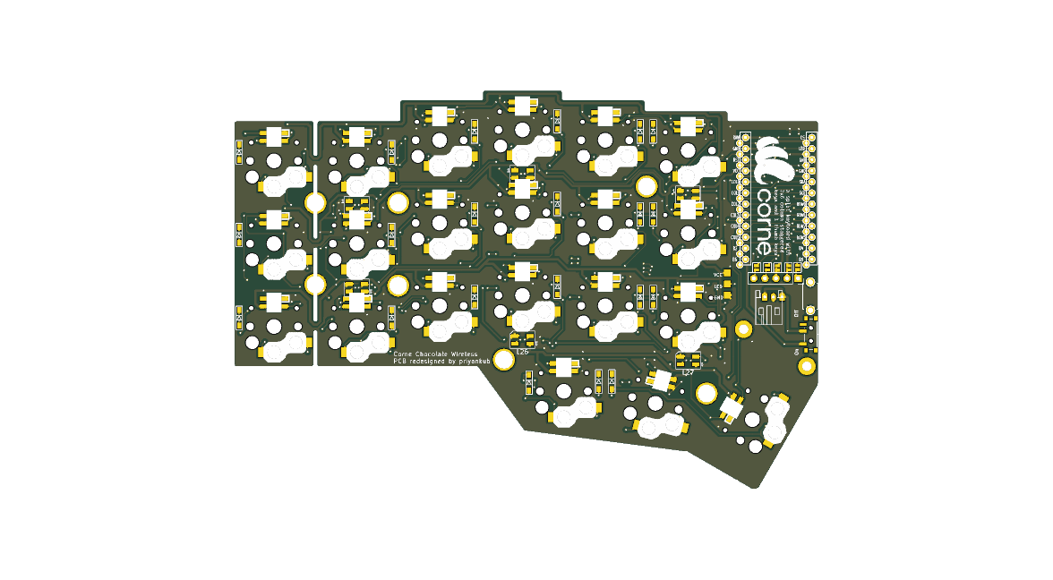
Corne chocolate is an open-source printed circuit board by priyankub, from the priyankub/corne repository on GitHub, published under the MIT licence. It is a 2-layer board of 133.8 × 91.4 mm with 104 parts on 83 nets, routed with 2,966 tracks and 403 vias.
It is built around the SK6812MINI-E. Its parts include 33 inductors, 23 switches, 21 diodes, 4 connectors and 1 IC. It belongs with the keyboards and input and lEDs and displays boards and the AVR (ATmega, ATtiny) boards of this library.
A modern, low-profile split ergonomic keyboard based on the Corne (crkbd) Chocolate v2.1 footprint. Designed for completely wireless operation with nice!nano v2, native 5-pin nice!view (Sharp Memory LCD) support, onboard power management, and RGB backlighting.
[CS, MOSI, SCK, VCC, GND]) without adapter boards or bodge wires.RAW pin.CS).| Signal | nice!nano Pin | nRF Pin | Function |
|---|---|---|---|
| CS | 1 (TX0 / D1) | P0.06 | Display Chip Select |
| LED | 2 (RX1 / D0) | P0.08 | WS2812 RGB Data |
| SDA / MOSI | 3 (D2) | P0.17 | Display MOSI / I2C SDA |
| SCL / SCK | 4 (D3) | P0.20 | Display SCK / I2C SCL |
| RAW | 24 | — | Battery positive (switched via power slide switch) |
Viewed from the front (component side) with header pins at the bottom:
Pin:    [ 1 ]      [ 2 ]      [ 3 ]      [ 4 ]      [ 5 ]
Signal:  CS        MOSI       SCK        VCC        GND
(P0.06) (P0.17) (P0.20) (3.3V)Because the PCB is reversible, you bridge the 5 solder jumpers on the top (active) side of each half to route the display signals:
Left Hand (Top / Front side facing up):
Solder jumpers JP1 through JP5 on the front layer (F.Cu).
JP5 $\rightarrow$ Pin 1 (CS)JP4 $\rightarrow$ Pin 2 (MOSI / SDA)JP3 $\rightarrow$ Pin 3 (SCK / SCL)JP2 $\rightarrow$ Pin 4 (VCC)JP1 $\rightarrow$ Pin 5 (GND)Right Hand (Bottom / Back side facing up):
Solder jumpers JP6 through JP10 on the back layer (B.Cu).
JP6 $\rightarrow$ Pin 1 (CS)JP7 $\rightarrow$ Pin 2 (MOSI / SDA)JP8 $\rightarrow$ Pin 3 (SCK / SCL)JP9 $\rightarrow$ Pin 4 (VCC)JP10 $\rightarrow$ Pin 5 (GND)[!TIP] Only solder the jumpers on the top side of each half. Leave the jumpers on the underside unbridged.
Ready-to-manufacture files are located in hardware/production/:
| File | Description |
|---|---|
Corne_Chocolate_2.1.zip | Complete Gerber & Drill archive (JLCPCB / PCBWay ready) |
bom.csv | Bill of Materials with footprint designators |
positions.csv | Pick & Place (CPL) component coordinates |
netlist.ipc | IPC-D-356 electrical test netlist |
The repository includes a battle-tested ZMK setup under firmware/:
P0.08 for the WS2812 LED chain, preserving P0.06 for display CS.Build using the included GitHub Actions workflow or locally with the ZMK toolchain:
west build -b nice_nano//zmk -d build/left -- -DSHIELD="corne_left nice_view_adapter nice_epaper"
west build -b nice_nano//zmk -d build/right -- -DSHIELD="corne_right nice_view_adapter nice_epaper".
├── hardware/ # KiCad 9 PCB and Schematic source files
│ ├── corne-chocolate.kicad_pro
│ ├── corne-chocolate.kicad_sch
│ ├── corne-chocolate.kicad_pcb
│ ├── corne-chocolate.step
│ ├── kbd/ # KiCad symbol & footprint libraries
│ └── production/ # Gerbers, Drill, BOM, and CPL files
└── firmware/ # ZMK configuration & build recipes
├── config/ # corne.keymap and corne.conf
└── build.yaml # GitHub Actions matrix configurationIf you are working with an early prototype PCB printed before September 2026 (which had the display header signals routed in reverse order), you can run thin enamel jumper wires across the solder pads on the front of the left half instead of reprinting:
JP5 Pad 2 (Screen Pin 1 / CS) $\rightarrow$ Wire to JP1 Pad 1JP4 Pad 2 (Screen Pin 2 / MOSI) $\rightarrow$ Wire to JP5 Pad 1JP3 Pad 2 (Screen Pin 3 / SCK) $\rightarrow$ Wire to JP4 Pad 1JP2 Pad 2 (Screen Pin 4 / VCC) $\rightarrow$ Wire to JP3 Pad 1JP1 Pad 2 (Screen Pin 5 / GND) $\rightarrow$ Wire to JP2 Pad 1The files currently in this repository have this issue resolved natively in copper.
| Qty | Value | Footprint | References |
|---|---|---|---|
| 21 | D | kbd:D3_SMD | D1, D2, D3, D4, D10, D11, D12, D13, D14, D15, D16, D17, D18, D19, D20, D21 +5 |
| 21 | SK6812MINI | kbd:SK6812MINI_rev | L1, L2, L3, L4, L10, L11, L12, L13, L14, L15, L16, L17, L18, L19, L20, L21 +5 |
| 20 | SW_PUSH | kbd:Choc_Hotswap | SW1, SW2, SW3, SW4, SW5, SW10, SW11, SW12, SW13, SW14, SW15, SW16, SW17, SW18, SW19, SW20 +4 |
| 12 | SK6812MINI | LED_SMD:LED_SK6812MINI_PLCC4_3.5x3.5mm_P1.75mm | L22, L22, L23, L23, L24, L24, L25, L25, L26, L26, L27, L27 |
| 10 | ~ | kbd:Jumper | JP1, JP2, JP3, JP4, JP5, JP6, JP7, JP8, JP9, JP10 |
| 9 | kbd:LEGO_HOLE | , , , , , , , , | |
| 2 | BAT | Connector_JST:JST_PH_S2B-PH-K_1x02_P2.00mm_Horizontal | J1, J1 |
| 2 | LOGO | kbd:corne | G***, G*** |
| 2 | SW_SPDT | Button_Switch_SMD:SW_SPDT_PCM12 | SW22, SW23 |
| 1 | LED | kbd:StripLED_rev | J3 |
| 1 | OLED | Connector_PinSocket_2.54mm:PinSocket_1x05_P2.54mm_Vertical | J2 |
| 1 | ProMicro | kbd:ProMicro_v2 | U1 |
| 1 | SW_PUSH | kbd:ResetSW | RSW1 |
| 1 | SW_PUSH | kbd:Choc_Hotswap_1.5u | SW21 |
It measures 133.8 × 91.4 mm and has 2 copper layers, 1.6 mm thick.
104 parts, built around the SK6812MINI-E. The full list of its parts is on this page, with links to each part's symbol and footprint where PCBKit's library has them.
From the priyankub/corne repository on GitHub, at the commit this page was made from: the board is hardware/corne-chocolate.kicad_pcb and its schematic hardware/corne-chocolate.kicad_sch. PCBKit opens the board in the browser, with nothing to install.
Its repository publishes it under the MIT licence: you may reuse it on that licence's terms (keep the author's notice, and for a copyleft licence share your changes alike).
google/mozc-devices
Circuit diagrams and firmware source code for Gboard DIY keyboards

Bastardkb/Dilemma
The Dilemma is a vertical stagger low-profile keyboard with mods.

Pwnsat/FlatSat
Flatsat v1.0 is a hardware based platform for aerospace cybersecurity research

adamws/kicad-kbplacer
KiCad plugin for automatic keyboard's key placement and routing

imchipwood/dumbpad
Simple 4x4 numpad with rotary encoder. Powered by QMK via ATmega32u4 Pro Micro

makerforgetech/modular-biped
An open source framework for creating a bipedal modular companion robot.

