camera-gpio-interface-pcb
Interface board for the three FLIR Blackfly S cameras in the Janelia Dudman lab
joystick rig: pluggable screw-terminal camera connectors, two BNC inputs from
the pyControl breakout, four 3.3 V BNC outputs to a Neuropixels OneBox, an
InstrumentPort-Digital-50 with every camera line tapped, and USB power. No
MCU, no firmware, no configuration jumpers.
Status, October 2026: v1.0 is the fabricated revision. Five assembled
boards were ordered from JLCPCB on 2026-09-26
(fabrication log), and one is installed in the
rig, wired to the three cameras, the pyControl breakout and the OneBox. Bench
results per board go in the bring-up log.
The Board
The block below is written by make docs from the KiCad sources: renders, key
dimensions, and links to the schematic, BOM, STEP model and enclosure geometry.
Do not edit between the markers; run make docs instead.
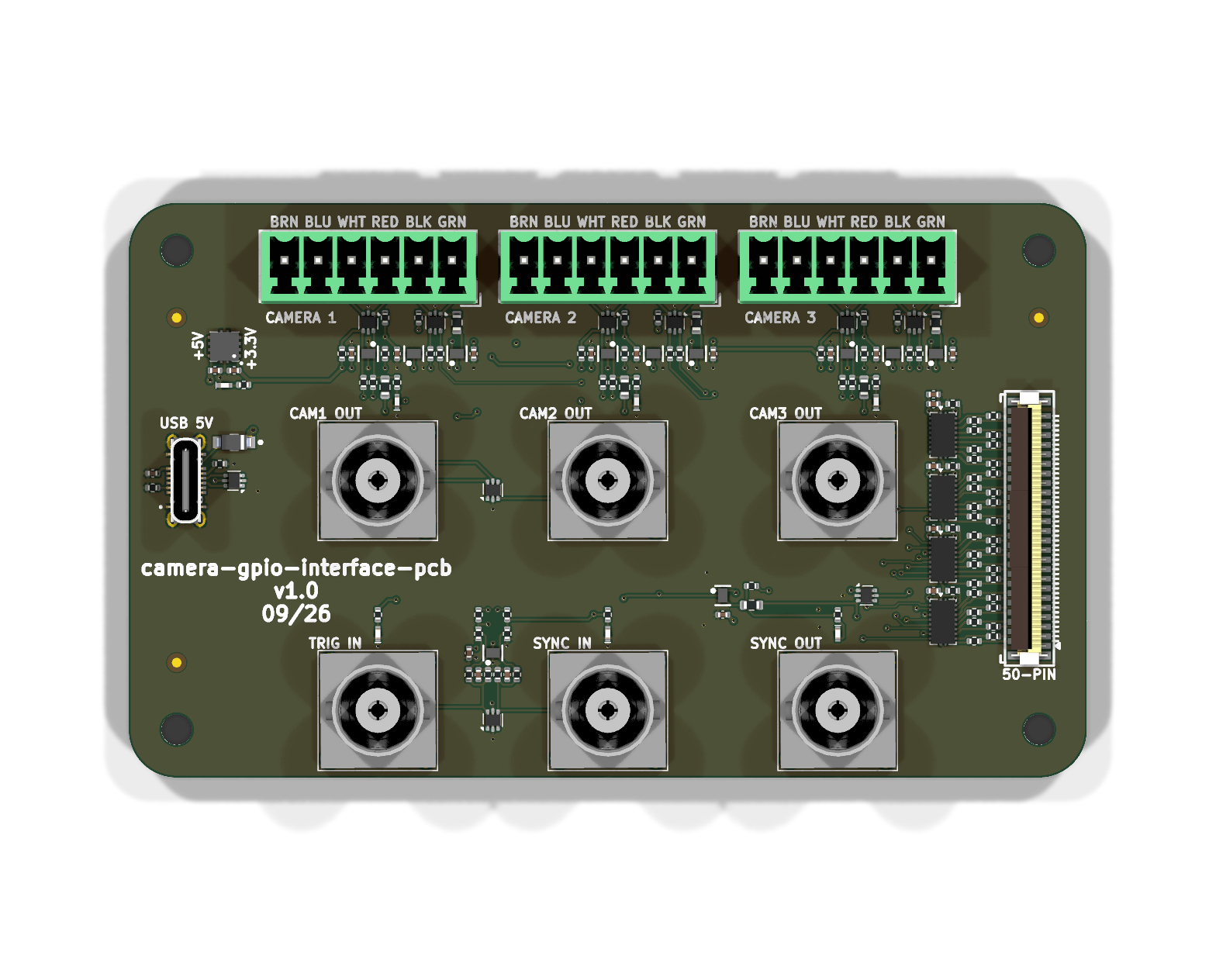
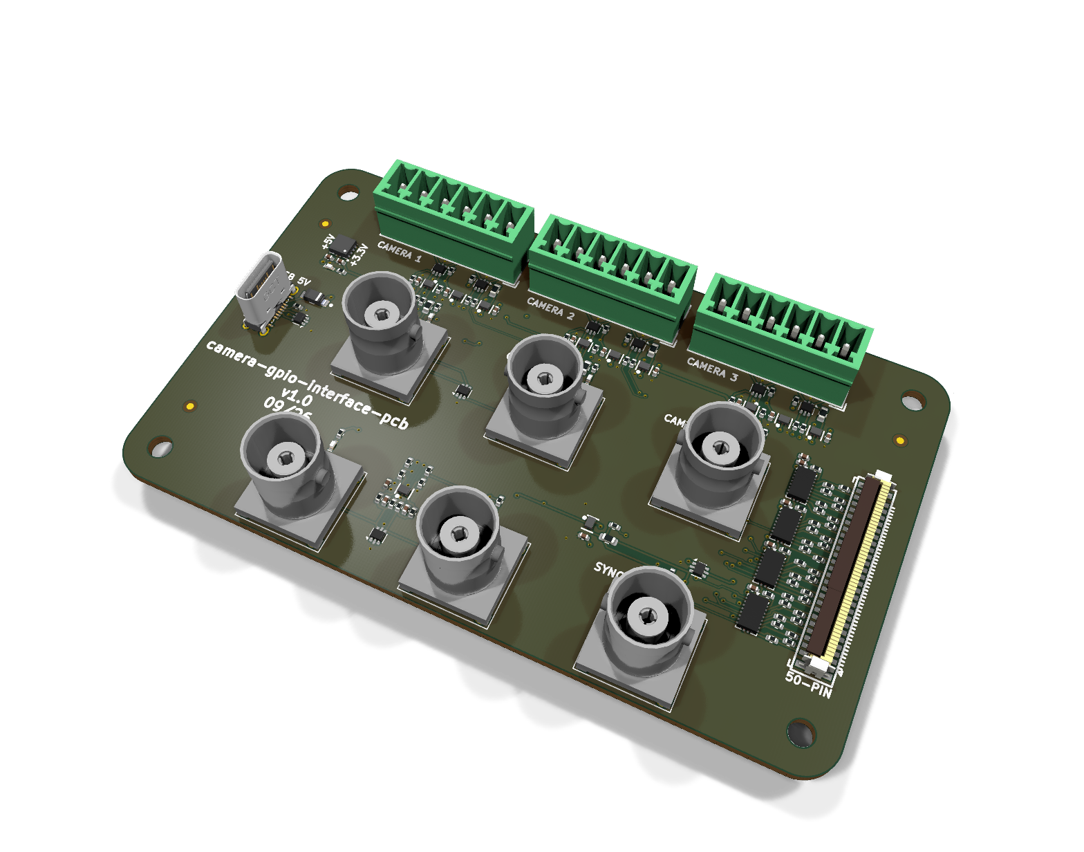
More views, including both elevations, are in the generated documentation.
The documentation site, with the board turning and its design blocks clickable: https://peterpolidoro.github.io/camera-gpio-interface-pcb/.
| Property | Value |
|---|
| Outline | 100.0 × 60.0 mm, 5.0 mm corner radius |
| Thickness | 1.6 mm |
| Copper layers | 4 |
| Mounting holes | 4 × 3.2 mm |
| Connectors and controls | 11 |
| Bill of materials | 26 distinct parts, 151 placements |
Documents
| Document | File |
|---|
| Schematic, all sheets, PDF | camera-gpio-interface-pcb-schematic.pdf |
| Schematic sheets, SVG (11) | schematic/ |
| Schematic, instance overviews and details, PDF | Review booklet |
| Design blocks placed (7), one page each | blocks/README.md |
| Board view: the model and the top render with the design blocks numbered | board-view.md |
| Subsystem sheets (3), from their recipes | subsystems/README.md |
| Assembly view, top | assembly-top.svg |
| Assembly view, bottom | assembly-bottom.svg |
| Assembled board, STEP, for FreeCAD | camera-gpio-interface-pcb-assembled.step |
| Assembled board, glTF, for a viewer (the library's materials written in) | camera-gpio-interface-pcb.glb |
| Bill of materials | table · CSV |
| Outline and mounting holes, dimensioned drawing | SVG · PDF · PNG |
| Board dimensions and stackup | board-dimensions.md |
| Board geometry, machine readable | board-geometry.json |
| Mounting holes | mounting-holes.csv |
| Connector locations | connectors.csv |
Enclosure Reference
Millimetres from the centre of the board outline, X right and Y up,
looking at the top of the board. Extents are the part's courtyard, which is
what a panel cutout has to clear. Full tables in board-dimensions.md.
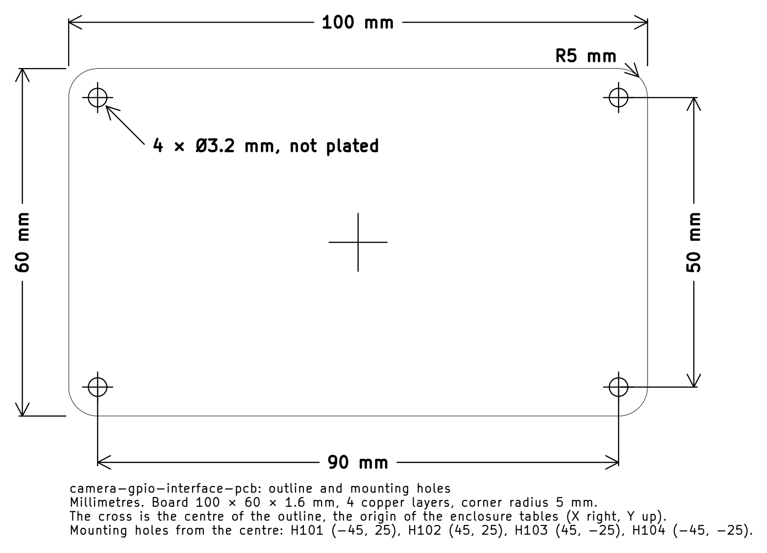
The outline and the mounting holes dimensioned, as KiCad draws them: SVG · PDF; the cross is the centre the tables measure from.
Mounting holes
| Ref | X (mm) | Y (mm) | Drill (mm) |
|---|
| H101 | -45.0 | 25.0 | 3.2 |
| H102 | 45.0 | 25.0 | 3.2 |
| H103 | 45.0 | -25.0 | 3.2 |
| H104 | -45.0 | -25.0 | 3.2 |
Connectors and controls
| Ref | Part | X (mm) | Y (mm) | Rot | Extent X (mm) | Extent Y (mm) |
|---|
| J301 | HL-BNC-KHDA | -24.0 | -23.0 | 0.0 | -30.5 to -17.5 | -29.5 to -16.5 |
| J302 | HL-BNC-KHDA | 0.0 | -23.0 | 0.0 | -6.5 to 6.5 | -29.5 to -16.5 |
| J401 | HL-BNC-KHDA | 24.0 | -23.0 | 0.0 | 17.5 to 30.5 | -29.5 to -16.5 |
| J402 | HL-BNC-KHDA | -24.0 | 1.0 | 0.0 | -30.5 to -17.5 | -5.5 to 7.5 |
| J403 | HL-BNC-KHDA | 0.0 | 1.0 | 0.0 | -6.5 to 6.5 | -5.5 to 7.5 |
| J404 | HL-BNC-KHDA | 24.0 | 1.0 | 0.0 | 17.5 to 30.5 | -5.5 to 7.5 |
| J501 | FH12-50S-0.5SVA(54) | 44.0 | -4.0 | 270.0 | 41.2 to 46.8 | -18.75 to 10.75 |
| J701 | TBH-1x06-3.5mm | -25.0 | 24.0 | 180.0 | -36.7 to -13.3 | 19.25 to 27.5 |
| J901 | USB-C | -44.0 | 1.0 | 90.0 | -46.31 to -41.69 | -4.05 to 6.05 |
| J1201 | TBH-1x06-3.5mm | 0.0 | 24.0 | 180.0 | -11.7 to 11.7 | 19.25 to 27.5 |
| J1401 | TBH-1x06-3.5mm | 25.0 | 24.0 | 180.0 | 13.3 to 36.7 | 19.25 to 27.5 |
Documents
- Interface map: what each connector and instrument-port channel carries
- Rev 0 plan: the design record
- Fabrication log: what was ordered, from which commit, with which package hashes
- Bring-up log: bench results per board serial
- Generated board documentation: schematic PDF and SVGs, renders, STEP and glTF, BOM, enclosure geometry and the dimensioned outline drawing, one page per placed design block and per subsystem sheet, rebuilt from the KiCad sources
- The documentation site: the same pages with the board turning and its design blocks clickable
Fabrication
The v1.0 boards were ordered assembled from JLCPCB from the package built at
commit 5ddb425. The fabrication log records the
commit, the source hashes and the hash of every file JLCPCB received.
fab/camera-gpio-interface-pcb/ holds the
package rebuilt from the same sources on 2026-10-12: upload
camera-gpio-interface-pcb-jlcpcb.zip, jlcpcb-bom.csv and
jlcpcb-camera-gpio-interface-pcb-all-pos.csv to order more boards. The BOM
and placement files are byte-identical to the uploaded ones; the gerbers
differ only by the creation time in their headers. To fabricate elsewhere,
plot the layers and drill files from kicad/camera-gpio-interface-pcb.kicad_pcb
in KiCad. JLCPCB's placement rotation differs from KiCad's for some
footprints, so check the assembly preview before confirming an order.
Related Repositories
- mouse-joystick-pcb: the rig's joystick controller board.
- mouse-joystick-firm: its firmware and the pyControl device class.
- mouse-joysticks-mech: the two-joystick mechanical assembly, part by part, with the atlas site and the PDF manual of the whole rig.
- joystick-rig: the rig's pyControl tasks, hardware definition and operating notes.
Development
Opening, editing and fabricating the board needs only KiCad 10; the schematic
and board carry their own copies of every symbol and footprint. The board was
drawn from a shared KiCad library and toolchain, which is needed only to
regenerate docs/generated/, the fabrication package or the composed sheets.
docs/development.md describes that toolchain, the
environment, the sibling repositories and the layout record. Agent guidance is
in AGENTS.md and .agents/.
License
Hardware design files and documentation are CC-BY-SA-4.0; code and automation
are 3-clause BSD. See LICENSE.
Citation
CITATION.cff carries the citation metadata; GitHub renders it
under "Cite this repository".


