2 layers176.6 × 97.8 mm
 PercyJW-2/Split652
Split 65 Percent Keyboard
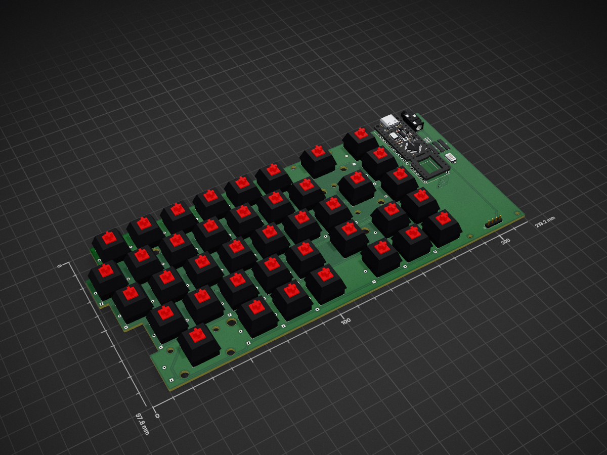
Split65Right is an open-source printed circuit board by PercyJW-2, from the PercyJW-2/Split65 repository on GitHub, published under the MIT licence. It is a 2-layer board of 219.2 × 97.8 mm with 97 parts on 80 nets, routed with 401 tracks and 26 vias.
Its parts include 40 diodes, 40 switches, 3 resistors, 2 connectors and 1 IC.
Split 65 Percent Keyboard


| Qty | Value | Footprint | References |
|---|---|---|---|
| 40 | D | footprints:D_SOD123_axial | D1, D2, D10, D11, D12, D13, D14, D15, D16, D17, D18, D19, D20, D21, D22, D23 +24 |
| 36 | SW_PUSH | footprints:KailhSocket-1U | SW1, SW10, SW11, SW12, SW13, SW14, SW15, SW16, SW17, SW19, SW20, SW21, SW22, SW23, SW24, SW25 +20 |
| 4 | VAL** | footprints:HOLE_M2_TH | HOLE_3M, HOLE_3M, HOLE_3M, HOLE_3M |
| 4 | VAL** | footprints:HOLE_M2 | HOLE_M2, HOLE_M2, HOLE_M2, HOLE_M2 |
| 2 | 5k | footprints:R_1608_axial | R1, R2 |
| 2 | GND | footprints:Jumper | JP2, JP3 |
| 1 | 120 | footprints:R_1608_axial | R3 |
| 1 | Jack4 | footprints:TRRS_JACK_MJ4PP9 | J1 |
| 1 | OLED | footprints:OLED_4Pin | J2 |
| 1 | Proton_C | footprints:proton_c | U1 |
| 1 | SW_PUSH | footprints:KailhSocket-ISO | SW18 |
| 1 | SW_PUSH | footprints:KailhSocket-2.25U | SW39 |
| 1 | SW_PUSH | footprints:KailhSocket-1.75U | SW27 |
| 1 | SW_PUSH | footprints:KailhSocket-2U | SW2 |
| 1 | SW_Push | footprints:TACT_SWITCH_TVBP06 | SW_41 |
It measures 219.2 × 97.8 mm and has 2 copper layers, 1.6 mm thick.
97 parts. The full list of its parts is on this page, with links to each part's symbol and footprint where PCBKit's library has them.
From the PercyJW-2/Split65 repository on GitHub, at the commit this page was made from: the board is Split65Right.kicad_pcb. PCBKit opens the board in the browser, with nothing to install.
Its repository publishes it under the MIT licence: you may reuse it on that licence's terms (keep the author's notice, and for a copyleft licence share your changes alike).


freeDSP/freeDSP-aurora
freeDSP ADAU1452 with 8 analog input, 8 analog outputs, S/P-DIF I/O, ADAT I/O, USB Audio Class2, WiFi, Bluetooth

matthewcieplak/super-sixteen
Code and schematics for the Super Sixteen Eurorack sequencer

ZeroPhone/ZeroPhone-PCBs
PCB files for ZeroPhone - for gerbers and schematics, go to "Releases" tab!


cnlohr/cnhardware
My dumping grounds for all my kicad projects and random hardware bringup.