
2 layers29.2 × 39 mm
Ch32-devboard
parammakersadda/CH32-devBoard
a simple development board based on CH32X033F8P6 microcontroller
22 partsCERN-OHL-W-2.0

 parammakersadda/CH32-devBoard
a simple development board based on CH32X033F8P6 microcontroller
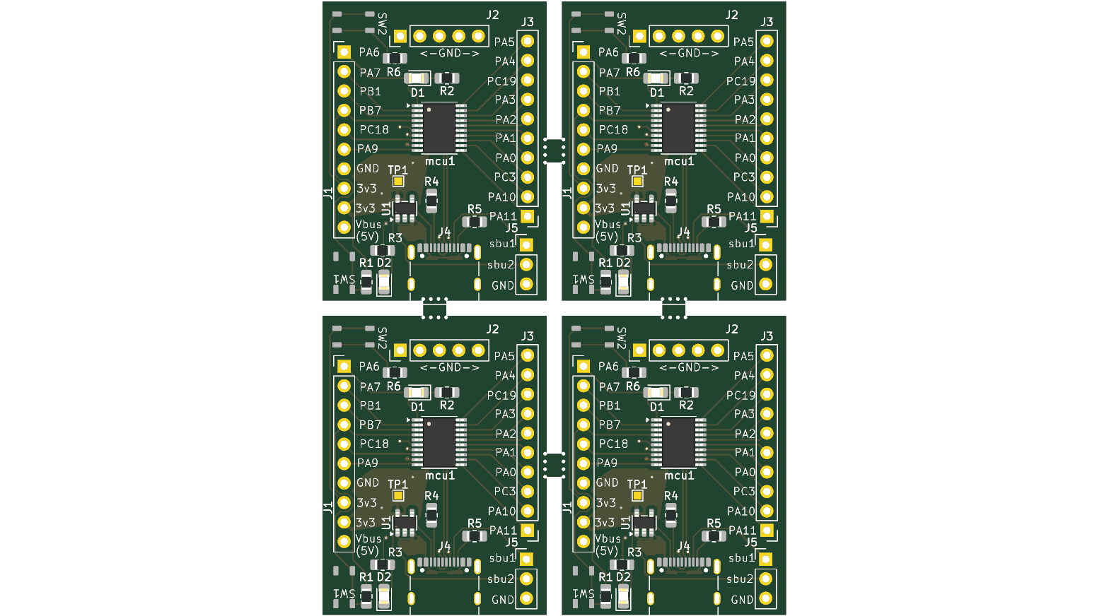
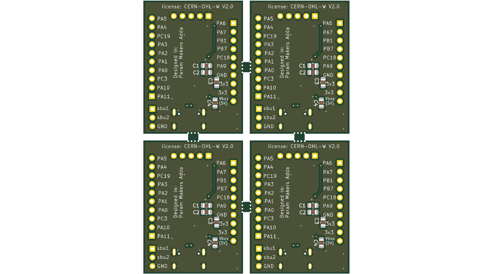
Panelised pcb is an open-source printed circuit board by parammakersadda, from the parammakersadda/CH32-devBoard repository on GitHub, published under the CERN-OHL-W-2.0 licence. It is a 2-layer board of 60.4 × 80 mm with 120 parts on 112 nets, routed with 588 tracks and 80 vias.
It is built around the AP2112K-3.3. Its parts include 24 resistors, 20 connectors, 16 capacitors, 8 diodes and 8 switches. It belongs with the microcontroller boards boards of this library.
This directory contains the panelized PCB design for the CH32 development board.
Panelization is automated using KiKit through a KiCad Jobset.
.kicad_jobset).The panelized PCB will be generated automatically.
front
 back
 routing
| Qty | Value | Footprint | References |
|---|---|---|---|
| 32 | NPTH | NPTH | KiKit_MB_1_1, KiKit_MB_1_2, KiKit_MB_1_3, KiKit_MB_1_4, KiKit_MB_2_1, KiKit_MB_2_2, KiKit_MB_2_3, KiKit_MB_2_4, KiKit_MB_3_1, KiKit_MB_3_2, KiKit_MB_3_3, KiKit_MB_3_4, KiKit_MB_4_1, KiKit_MB_4_2, KiKit_MB_4_3, KiKit_MB_4_4 +16 |
| 8 | 10k | Resistor_SMD:R_0805_2012Metric_Pad1.20x1.40mm_HandSolder | R1, R1, R1, R1, R6, R6, R6, R6 |
| 8 | 1k | Resistor_SMD:R_0805_2012Metric_Pad1.20x1.40mm_HandSolder | R2, R2, R2, R2, R3, R3, R3, R3 |
| 8 | 4.7uF | Capacitor_SMD:C_0805_2012Metric_Pad1.18x1.45mm_HandSolder | C3, C3, C3, C3, C4, C4, C4, C4 |
| 8 | 5.1k | Resistor_SMD:R_0805_2012Metric_Pad1.20x1.40mm_HandSolder | R4, R4, R4, R4, R5, R5, R5, R5 |
| 8 | Conn_01x10_Pin | Connector_PinHeader_2.54mm:PinHeader_1x10_P2.54mm_Vertical | J1, J1, J1, J1, J3, J3, J3, J3 |
| 8 | LED | LED_SMD:LED_0805_2012Metric_Pad1.15x1.40mm_HandSolder | D1, D1, D1, D1, D2, D2, D2, D2 |
| 8 | SW_Push | ch32-devBoard-symbols:smd-push-button-TS3425PA | SW1, SW1, SW1, SW1, SW2, SW2, SW2, SW2 |
| 4 | 0.1uF | Capacitor_SMD:C_0805_2012Metric_Pad1.18x1.45mm_HandSolder | C1, C1, C1, C1 |
| 4 | 1uF | Capacitor_SMD:C_0805_2012Metric_Pad1.18x1.45mm_HandSolder | C2, C2, C2, C2 |
| 4 | AP2112K-3.3 | Package_TO_SOT_SMD:SOT-23-5 | U1, U1, U1, U1 |
| 4 | Conn_01x03_Socket | Connector_PinHeader_2.54mm:PinHeader_1x03_P2.54mm_Vertical | J5, J5, J5, J5 |
| 4 | Conn_01x05_Pin | Connector_PinHeader_2.54mm:PinHeader_1x05_P2.54mm_Vertical | J2, J2, J2, J2 |
| 4 | USB_C_Receptacle_USB2.0_16P | Connector_USB:USB_C_Receptacle_Palconn_UTC16-G | J4, J4, J4, J4 |
| 4 | VDD(3v3) | TestPoint:TestPoint_Pad_1.0x1.0mm | TP1, TP1, TP1, TP1 |
| 4 | ~ | Package_SO:TSSOP-20_4.4x6.5mm_P0.65mm | mcu1, mcu1, mcu1, mcu1 |
parammakersadda/CH32-devBoard
a simple development board based on CH32X033F8P6 microcontroller

FrameworkComputer/ExpansionCards
Reference designs and documentation to create Expansion Cards for the Framework Laptop


DDeGonge/OS-ARM
This arm is not industrial and it will not be fast, but that is not my goal. But it will hopefully be a very nice looking arm fully capable of 6dof motion, cheap enough to keep it accessable but capable enough to…


It measures 60.4 × 80 mm and has 2 copper layers, 1.6 mm thick.
120 parts, built around the AP2112K-3.3. The full list of its parts is on this page, with links to each part's symbol and footprint where PCBKit's library has them.
From the parammakersadda/CH32-devBoard repository on GitHub, at the commit this page was made from: the board is panelisedPcb/panelised-pcb.kicad_pcb and its schematic ch32-devboard.kicad_sch. PCBKit opens the board in the browser, with nothing to install.
Its repository publishes it under the CERN-OHL-W-2.0 licence: you may reuse it on that licence's terms (keep the author's notice, and for a copyleft licence share your changes alike).