
6 layers100.3 × 68.6 mm
MYRIAD RD 5.1.2.unrouted
aspdac-submission-pcb-layout/PCB-Layout-Framework
This repository has been prepared from the original. Some care has been taken to remove the names of the authors.
984 parts7BSD-3-Clause
 oscimp/oscimpDigital59
OscillatorIMP ecosystem for the digital characterization of ultrastable oscillators and Software Defined Radio (SDR) frontend processing
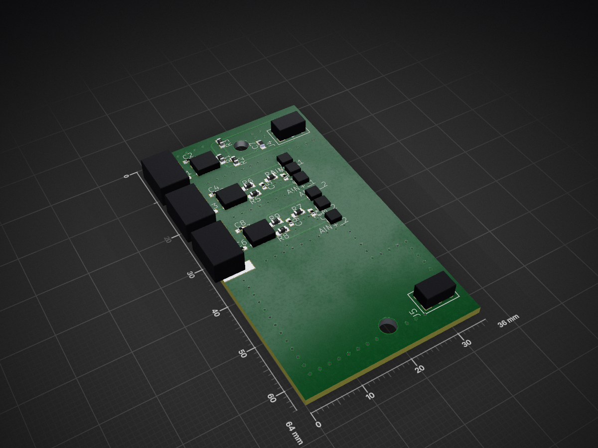
Extension clk adc is an open-source printed circuit board by oscimp, from the oscimp/oscimpDigital repository on GitHub. It is a 2-layer board of 36 × 64 mm with 34 parts on 27 nets, routed with 148 tracks and 94 vias.
It is built around the TC1-1-13MA+. Its parts include 11 capacitors, 9 resistors and 5 connectors. It belongs with the radio and wireless and fPGA and programmable logic boards and the FPGA and CPLD boards of this library.
Hardware modifications of the 14-bit Red Pitaya (also known as STEMlab 125-14) described in report.pdf, and the associated KiCAD files (courtesy of Gilles Martin, FEMTO-ST, France, translated from Eagle) for undersampling by getting rid of the unbalanced-balanced amplifier also acting as low pass filter.
For external clocking (125 MHz), only populate the balun and channel closest to the border of the PCB. The other two channels are for undersampling by bypassing the unbalanced to balanced differential amplifiers. Follow these instructions for wiring modifications (two resistors to be flipped) to disconnect the quartz crystal oscillator and connect the clock input to the PCLK external source pins.
Replacing the active amplifier with a broadband balun (tested over the whole track-and-hold range up to 875 MHz input frequency) requires soldering three tiny wires (differential pair and Vref) on each channel at your own risks after removing the inductors connecting the differential amplifier output to the ADC inputs. The Vref signal trace must be cut before soldering a wire to the via pad whose varnish will have been removed with a sharp blade.
| Qty | Value | Footprint | References |
|---|---|---|---|
| 10 | 100nF | extension_clk_adc:C0402 | C1, C2, C3, C4, C5, C6, C8, C9, C10, C11 |
| 6 | SMD2 | extension_clk_adc:SMD1,27-2,54 | AIN-_1, AIN-_2, AIN+_1, AIN+_2, VCM_1, VCM_2 |
| 4 | 25 | extension_clk_adc:R0603 | R5, R6, R8, R9 |
| 3 | SMA_BORD | extension_clk_adc:SMA_BORD | J1, J2, J3 |
| 3 | TC1-1-13M | extension_clk_adc:AT224-1A | TR1, TR2, TR3 |
| 2 | 50 | extension_clk_adc:R0603 | R2, R3 |
| 2 | DBL_6 | extension_clk_adc:DBL6 | J4, J5 |
| 2 | R-US_R0603 | extension_clk_adc:R0603 | R4, R7 |
| 1 | 100 | extension_clk_adc:R0603 | R1 |
| 1 | 100nF | extension_clk_adc:C0603 | C7 |
It measures 36 × 64 mm and has 2 copper layers, 1.6 mm thick.
34 parts, built around the TC1-1-13MA+. The full list of its parts is on this page, with links to each part's symbol and footprint where PCBKit's library has them.
From the oscimp/oscimpDigital repository on GitHub, at the commit this page was made from: the board is doc/external_clock_and_undersampling_PCB/extension_clk_adc.kicad_pcb and its schematic doc/external_clock_and_undersampling_PCB/extension_clk_adc.kicad_sch. PCBKit opens the board in the browser, with nothing to install.
Its repository states no licence, so its author keeps all rights: ask oscimp before reusing the design.
aspdac-submission-pcb-layout/PCB-Layout-Framework
This repository has been prepared from the original. Some care has been taken to remove the names of the authors.


FrameworkComputer/ExpansionCards
Reference designs and documentation to create Expansion Cards for the Framework Laptop

mntmn/amiga2000-gfxcard
MNT VA2000, an Open Source Amiga 2/3/4000 Graphics Card (Zorro II/III), written in Verilog

hackclub/OnBoard
💡 Join 1,000 teenagers and make your first PCB with a $100 grant!


strangeparts/niubi-headphones
Flexible circuit board design for adding a headphone jack to an iPhone 7
