2 layers70 × 65 mm
Fluepdot
Fluepke/Fluepdot
Project for controlling Annax flipdot panels used by the Berliner Verkehrsbetriebe
116 parts17AGPL-3.0

 openUC2/UC2_Feather
This is the first attempt to create a unified UC2 Electronics Module based on the ESP32
UC2-electronics cube is an open-source printed circuit board by openUC2, from the openUC2/UC2_Feather repository on GitHub. It is a 2-layer board of 170 × 50 mm with 74 parts on 78 nets, routed with 913 tracks and 547 vias.
It is built around the LP3321B6F, SS34 and SS14. Its parts include 18 diodes, 11 connectors, 9 resistors, 4 capacitors and 1 IC. It belongs with the ESP32 boards of this library.



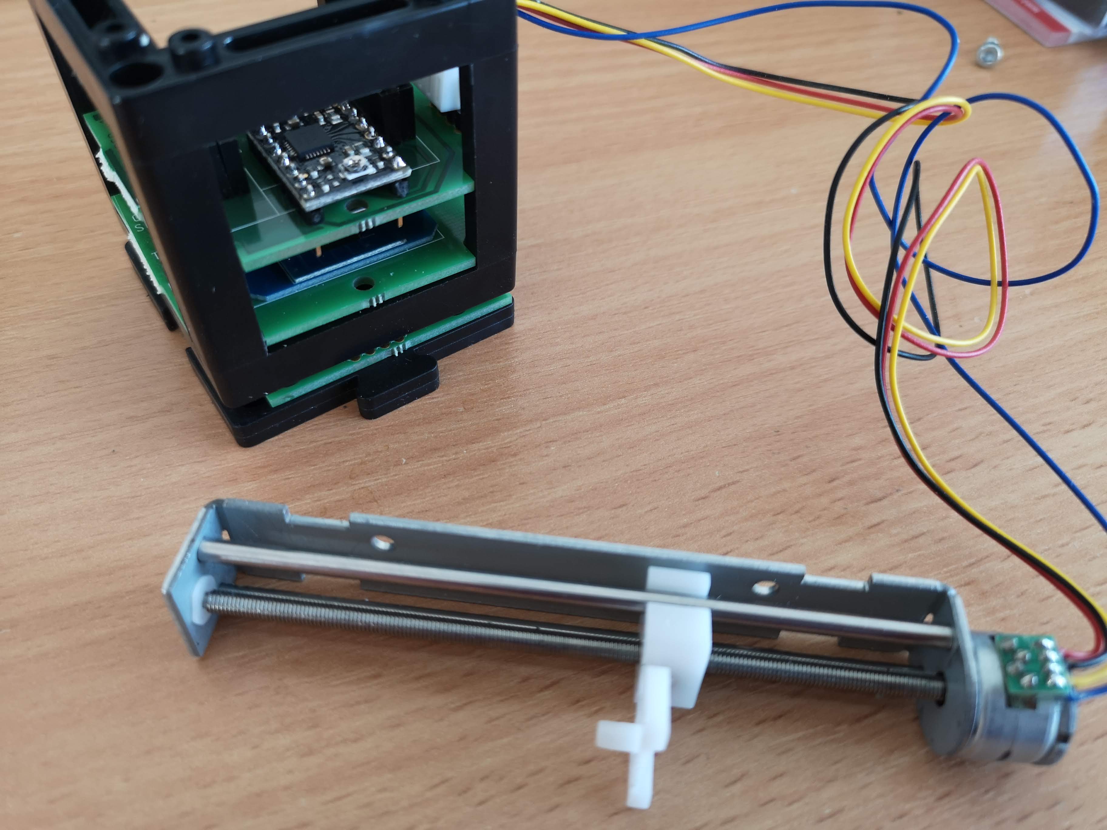
This is the second revision of the first attempt to have a unified modular electronics for the UC2 System. It was designed for UC2's "incubator microscope", a bright-field (transmission) microscope, which is the simplest type of microscope.
It consists of two boards:
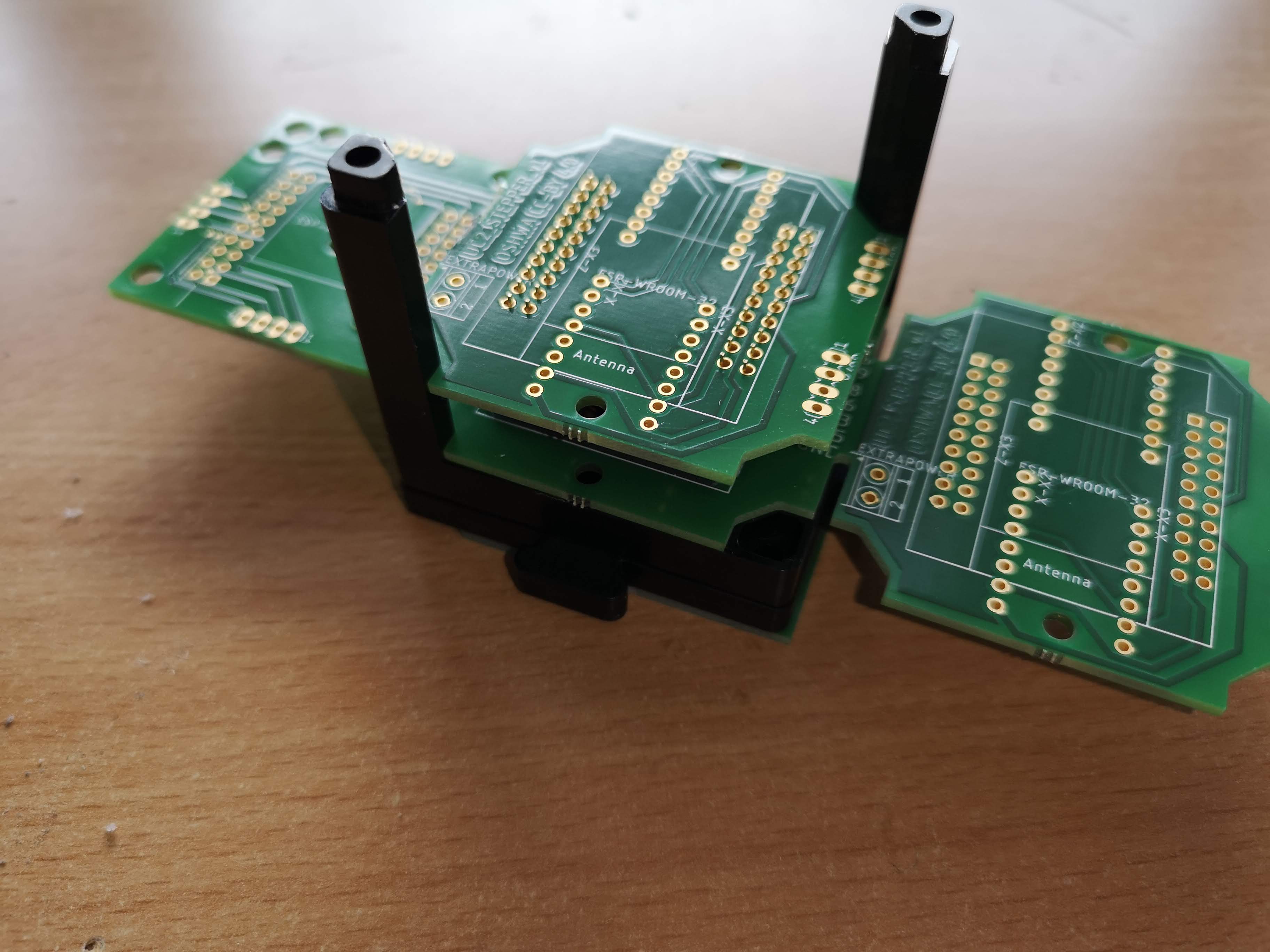
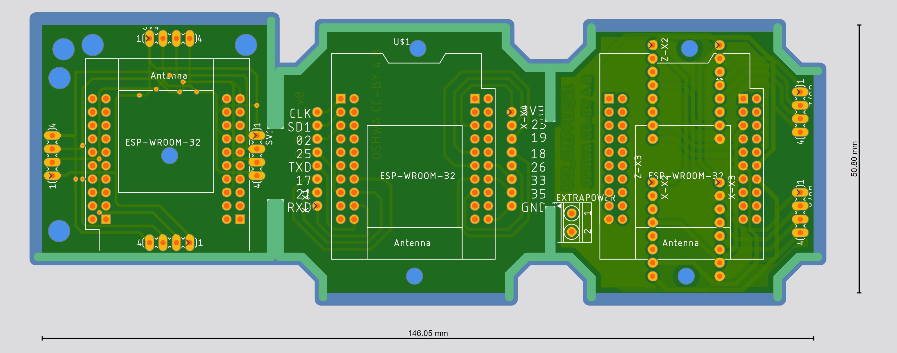
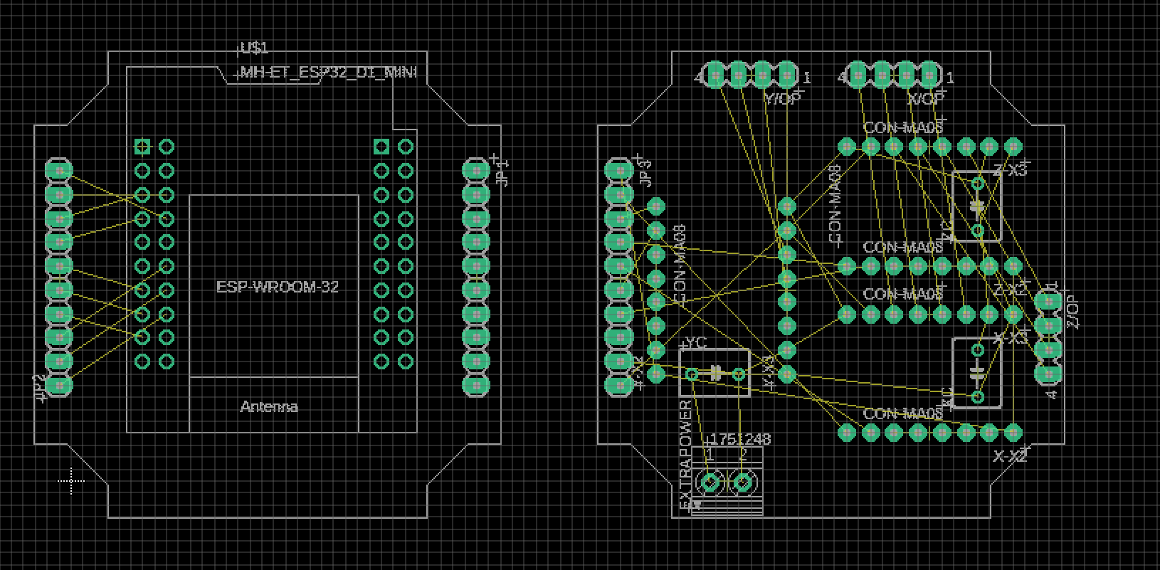
This PCB was created with KiCad 6. The board outline and safe zones (to let modules stick out the top of a cube) have been drawn in Inkscape (1.0.2) and then converted into a Kicad footprint with the svg2shenzhen plugin (0.2.18.7) for Inkscape.
We ordered it through TODO.
We will provide a unified Serial/WiFi-based REST API interface. A first version can be found in the https://github.com/openUC2/UC2-REST Repository.
This project is open so that anyone can get involved. You don't even have to learn CAD designing or programming. Find ways you can contribute in CONTRIBUTING
This project is open-source and is released under the CERN open hardware license. Our aim is to make the kits commercially available. We encourage everyone who is using our Toolbox to share their results and ideas, so that the Toolbox keeps improving. It should serve as a easy-to-use and easy-to-access general purpose building block solution for the area of STEAM education. All the design files are generally for free, but we would like to hear from you how is it going.
You're free to fork the project and enhance it. If you have any suggestions to improve it or add any additional functions make a pull-request or file an issue.
Please find the type of licenses here
REMARK: All files have been designed using Autodesk Inventor 2019 (EDUCATION)
If you find this project useful, please like this repository, follow us on Twitter and cite the webpage! :-)
| Qty | Value | Footprint | References |
|---|---|---|---|
| 16 | SS34 | Diode_SMD:D_SMA_Handsoldering | D301, D302, D303, D304, D305, D306, D307, D308, D401, D402, D403, D404, D405, D406, D407, D408 |
| 5 | 1R 1% | Resistor_SMD:R_0805_2012Metric | R202, R203, R204, R205, R206 |
| 2 | 100uF/6V | Capacitor_SMD:C_1206_3216Metric_Pad1.33x1.80mm_HandSolder | C301, C401 |
| 2 | 5.1k | Resistor_SMD:R_0805_2012Metric | R101, R102 |
| 2 | LOGO | lib:UC2-logo_halftoned | G***, G*** |
| 2 | LOGO | lib:oshw-number | G***, G*** |
| 2 | MS1_HIGH | Jumper:SolderJumper-2_P1.3mm_Bridged_RoundedPad1.0x1.5mm | JP302, JP402 |
| 2 | MS2_HIGH | Jumper:SolderJumper-2_P1.3mm_Bridged_RoundedPad1.0x1.5mm | JP303, JP403 |
| 2 | MS3_HIGH | Jumper:SolderJumper-2_P1.3mm_Bridged_RoundedPad1.0x1.5mm | JP304, JP404 |
| 2 | SLP-RST_NC | Jumper:SolderJumper-2_P1.3mm_Bridged_RoundedPad1.0x1.5mm | JP301, JP401 |
| 2 | STEMMA 3-pin jack | Connector_JST:JST_PH_S3B-PH-SM4-TB_1x03-1MP_P2.00mm_Horizontal | J104, J201 |
| 2 | daughterboard-simple-pins | Connector_PinHeader_2.54mm:PinHeader_1x03_P2.54mm_Vertical | J106, J203 |
| 2 | stepdrv_A4988 | Module:Pololu_Breakout-16_15.2x20.3mm | A301, A401 |
| 1 | 100k | Resistor_SMD:R_0805_2012Metric | R201 |
| 1 | 10uF/5V | Capacitor_SMD:C_0603_1608Metric | C201 |
| 1 | 3.3uH @ 1 MHz | L_SNR2010K_lib:SNR2010K | L201 |
| 1 | 39k | Resistor_SMD:R_0805_2012Metric | R207 |
| 1 | ESP-pins-breakout | Connector_PinHeader_2.54mm:PinHeader_2x13_P2.54mm_Vertical_SMD | J101 |
| 1 | LED_3W | LED_lumileds-l150_lib:LED_Lumileds_L150_thermalvias | D202 |
| 1 | LED_ANODE | TestPoint:TestPoint_Pad_D1.0mm | TP201 |
| 1 | LED_FULL_ON | Jumper:SolderJumper-2_P1.3mm_Open_RoundedPad1.0x1.5mm | JP202 |
| 1 | LED_external | Connector_PinHeader_2.54mm:PinHeader_1x02_P2.54mm_Vertical | J202 |
| 1 | LED_internal | Jumper:SolderJumper-2_P1.3mm_Bridged_RoundedPad1.0x1.5mm | JP201 |
| 1 | LP3321B6F | Package_TO_SOT_SMD:SOT-23-6 | U201 |
| 1 | SS14 | Diode_SMD:D_SMA | D201 |
| 1 | USBC_5V_3A_input | Connector_USB:USB_C_Receptacle_HRO_TYPE-C-31-M-12 | J105 |
| 1 | Val** | svg2shenzhen:im-cube_orthagonal-internal-pcb_svg2shenzhen | Ref** |
| 1 | Val** | svg2shenzhen:im-cube_orthagonal-externaljacks-pcb_svg2shenzhen | Ref** |
| 1 | esp32-mh-et-live | ESP32_mini:ESP32_mini | A101 |
| 1 | min. 2.2uF/30V | Capacitor_SMD:C_0805_2012Metric | C202 |
| 1 | pow_3.3V | Connector_PinHeader_2.54mm:PinHeader_1x02_P2.54mm_Vertical | J108 |
| 1 | pow_5V | Connector_PinHeader_2.54mm:PinHeader_1x02_P2.54mm_Vertical | J107 |
| 1 | stepdrv1_1A | TestPoint:TestPoint_Pad_D1.0mm | TP105 |
| 1 | stepdrv1_1B | TestPoint:TestPoint_Pad_D1.0mm | TP101 |
| 1 | stepdrv1_1B-2B-1A-2A-NC | jst-xh-smd_lib:JST_XH_S5B-XH-SM4-TB_1x05-1MP_Horizontal | J102 |
| 1 | stepdrv1_2A | TestPoint:TestPoint_Pad_D1.0mm | TP103 |
| 1 | stepdrv1_2B | TestPoint:TestPoint_Pad_D1.0mm | TP107 |
| 1 | stepdrv2_1A | TestPoint:TestPoint_Pad_D1.0mm | TP106 |
| 1 | stepdrv2_1B | TestPoint:TestPoint_Pad_D1.0mm | TP102 |
| 1 | stepdrv2_1B-2B-1A-2A-NC | jst-xh-smd_lib:JST_XH_S5B-XH-SM4-TB_1x05-1MP_Horizontal | J103 |
| 1 | stepdrv2_2A | TestPoint:TestPoint_Pad_D1.0mm | TP104 |
| 1 | stepdrv2_2B | TestPoint:TestPoint_Pad_D1.0mm | TP108 |
The 72 most common of 74 parts.
It measures 170 × 50 mm and has 2 copper layers, 1.6 mm thick.
74 parts, built around the LP3321B6F, SS34 and SS14. The full list of its parts is on this page, with links to each part's symbol and footprint where PCBKit's library has them.
From the openUC2/UC2_Feather repository on GitHub, at the commit this page was made from: the board is kicad/UC2-electronics-cube/UC2-electronics-cube.kicad_pcb and its schematic kicad/UC2-electronics-cube/UC2-electronics-cube.kicad_sch. PCBKit opens the board in the browser, with nothing to install.
Its repository states no licence, so its author keeps all rights: ask openUC2 before reusing the design.
Fluepke/Fluepdot
Project for controlling Annax flipdot panels used by the Berliner Verkehrsbetriebe

4rynv/Eklavya_Gantry
an attempt to automate screwing out and in of screw holes arranged in a matrix formation

cc90202/DCC-esp32
DCC command station for ESP32-C6 — NMRA-compliant model railroad controller in Rust


m24h/esp2400
A digitalizing power supply control board woking with modified ZXD2400 (50V 50A) modoule

jayanta525/dual-h-bridge
Dual H-Bridge Controller with IRF3205 and IR2104 MOSFET Driver, and with ATMega328P-AU PWM Controller

shashwtd/Open-FlipDisk
an open source 5x5 flip-dot display module built around custom electromagnetic flip discs, a Raspberry Pi Pico 2 W, and a custom driver PCB.

DevKiDCosmo/SATELLITE-EDGE-MODULE
A satellite edge module ready for competition