2 layers177 × 35 mm

 cc90202/DCC-esp3212
DCC command station for ESP32-C6 — NMRA-compliant model railroad controller in Rust
Dcc station is an open-source printed circuit board by cc90202, from the cc90202/DCC-esp32 repository on GitHub. It is a 2-layer board of 100 × 120 mm with 82 parts on 56 nets, routed with 722 tracks and 309 vias.
It is built around the 74HC08D, 74HC14 and LM339, with the TPS54302, SS34 and AO4407A among its other parts. Its parts include 23 resistors, 16 capacitors, 12 connectors, 9 diodes and 4 ICs. It belongs with the ESP32 and RISC-V boards of this library.


The board of the DCC-esp32 command station: 100 x 120 mm, two layers, powered by an external 12–19 V adapter. A Waveshare ESP32-C6-Zero and a Pololu DRV8874 carrier plug into its sockets.
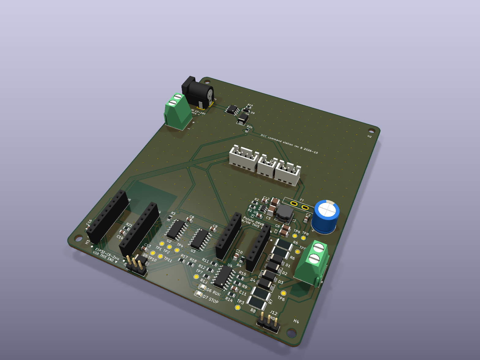
Rev B is the current design. It was built by JLCPCB and works on a 15 V bench supply on J9: power, ESP32, display, LEDs, Wi-Fi, DCC to the track and RailCom reads, and it starts with the display unplugged. Not tried yet: a reversed supply, the buttons, a 19 V supply and a short on the track.
Rev A (PR #41, commit ceebd3d) was built by JLCPCB and works on a 15 V bench supply: power, ESP32, display, LEDs, buttons, Wi-Fi, DCC to the track and RailCom reads. It carried a 230 V mains module on the board. Do not connect a rev A board to the mains: power it with 15 V on the module's output pins, as it was tested.
What rev B changes:
The CPL already carries the rotation corrections for JLCPCB's footprints; one exported again from KiCad would not.
Use a regulated adapter of 12 to 19 V, at least 2.5 A, with a 5.5 x 2.5 mm plug, centre positive, double insulated (Class II, the square-in-a-square symbol). Choose the voltage by scale: the track gets the adapter voltage minus about 1 V under load (bridge, clamp diodes, fuse), so 12 V for N and 15 V for H0.
A 5.5 x 2.1 mm plug goes into the 2.5 mm jack but makes poor contact; use the right plug.
Never use a 24 V adapter, even though it has the same plug. Nothing on the board is damaged by it, but the decoders would get 23 V, and the firmware does not check the input voltage yet.
For bench work, a bench supply can be connected to the screw terminal J9 ("+" and "−" on the silkscreen) instead of the adapter. Never use both at once: a bench supply set above the adapter would push current into it.
USB and the adapter can be connected at the same time.
J12, on the bottom edge right of the sense resistors, is three ground pins for an oscilloscope probe's ground clip.
fab/dcc-station.step is the 3D model of the assembled board, for designing a box. The barrel jack J1 sits on the left edge, where the box needs a round opening for the plug; C1 is 16 mm tall.
Open dcc-station.kicad_pro in KiCad 10. The symbol of Q1 (AO4407A) is in symbols/dcc.kicad_sym, the footprints of F1 and of the barrel jack J1 (pads from the XKB drawing) in footprints/dcc.pretty.
CERN Open Hardware Licence v2, strongly reciprocal (LICENSE).
| Qty | Value | Footprint | References |
|---|---|---|---|
| 11 | 100nF 50V X7R | Capacitor_SMD:C_0805_2012Metric | C2, C5, C8, C9, C10, C11, C12, C13, C14, C15, C16 |
| 5 | 1k | Resistor_SMD:R_0805_2012Metric | R9, R10, R14, R24, R25 |
| 4 | 10k | Resistor_SMD:R_0805_2012Metric | R4, R21, R22, R23 |
| 4 | 4.7R 1W | Resistor_SMD:R_2512_6332Metric | R5, R6, R7, R8 |
| 4 | M3 | MountingHole:MountingHole_3.2mm_M3 | H1, H2, H3, H4 |
| 4 | SS34 | Diode_SMD:D_SMA | D1, D2, D3, D4 |
| 2 | 100k | Resistor_SMD:R_0805_2012Metric | R3, R19 |
| 2 | 100k 1% | Resistor_SMD:R_0805_2012Metric | R1, R20 |
| 2 | 10uF 50V X7R | Capacitor_SMD:C_1210_3225Metric | C3, C4 |
| 2 | 22uF 25V | Capacitor_SMD:C_1206_3216Metric | C6, C7 |
| 2 | 470R | Resistor_SMD:R_0805_2012Metric | R17, R18 |
| 1 | 100R | Resistor_SMD:R_0805_2012Metric | R13 |
| 1 | 10uH 3A | Inductor_SMD:L_Bourns_SRN6045TA | L1 |
| 1 | 13.7k 1% | Resistor_SMD:R_0805_2012Metric | R2 |
| 1 | 22k | Resistor_SMD:R_0805_2012Metric | R11 |
| 1 | 4.7k | Resistor_SMD:R_0805_2012Metric | R12 |
| 1 | 470uF 35V | Capacitor_THT:CP_Radial_D10.0mm_P5.00mm | C1 |
| 1 | 74HC08 | Package_SO:SOIC-14_3.9x8.7mm_P1.27mm | U2 |
| 1 | 74HC14 | Package_SO:SOIC-14_3.9x8.7mm_P1.27mm | U3 |
| 1 | AO4407A | Package_SO:SOIC-8_3.9x4.9mm_P1.27mm | Q1 |
| 1 | BZT52C12 | Diode_SMD:D_SOD-123 | D9 |
| 1 | DC IN 12-19V | TerminalBlock_Phoenix:TerminalBlock_Phoenix_MKDS-1,5-2_1x02_P5.00mm_Horizontal | J9 |
| 1 | DC-005-5A-2.5 | dcc:BarrelJack_XKB_DC-005-5A | J1 |
| 1 | DISPLAY | Connector_JST:JST_XH_B4B-XH-A_1x04_P2.50mm_Vertical | J3 |
| 1 | ESP32-C6-Zero left row | Connector_PinSocket_2.54mm:PinSocket_1x09_P2.54mm_Vertical | J4 |
| 1 | ESP32-C6-Zero right row | Connector_PinSocket_2.54mm:PinSocket_1x09_P2.54mm_Vertical | J5 |
| 1 | GND SCOPE | Connector_PinHeader_2.54mm:PinHeader_1x03_P2.54mm_Vertical | J12 |
| 1 | LED green 0805 | LED_SMD:LED_0805_2012Metric | D6 |
| 1 | LED red 0805 | LED_SMD:LED_0805_2012Metric | D7 |
| 1 | LM339 | Package_SO:SOIC-14_3.9x8.7mm_P1.27mm | U4 |
| 1 | MF-R400 4A 30V | dcc:Polyfuse_Radial_P5.08mm_W14.5mm | F1 |
| 1 | Pololu DRV8874 #4035 left row | Connector_PinSocket_2.54mm:PinSocket_1x07_P2.54mm_Vertical | J6 |
| 1 | Pololu DRV8874 #4035 right row | Connector_PinSocket_2.54mm:PinSocket_1x07_P2.54mm_Vertical | J7 |
| 1 | RESUME | Connector_JST:JST_XH_B2B-XH-A_1x02_P2.50mm_Vertical | J10 |
| 1 | SERIAL TX RX GND | Connector_PinHeader_2.54mm:PinHeader_1x03_P2.54mm_Vertical | J8 |
| 1 | SMBJ24A | Diode_SMD:D_SMB | D8 |
| 1 | SS14 | Diode_SMD:D_SMA | D5 |
| 1 | STOP | Connector_JST:JST_XH_B3B-XH-A_1x03_P2.50mm_Vertical | J11 |
| 1 | TP1 | TestPoint:TestPoint_Pad_D1.5mm | TP1 |
| 1 | TP10 | TestPoint:TestPoint_Pad_D1.5mm | TP10 |
| 1 | TP11 | TestPoint:TestPoint_Pad_D1.5mm | TP11 |
| 1 | TP2 | TestPoint:TestPoint_Pad_D1.5mm | TP2 |
| 1 | TP3 | TestPoint:TestPoint_Pad_D1.5mm | TP3 |
| 1 | TP4 | TestPoint:TestPoint_Pad_D1.5mm | TP4 |
| 1 | TP5 | TestPoint:TestPoint_Pad_D1.5mm | TP5 |
| 1 | TP6 | TestPoint:TestPoint_Pad_D1.5mm | TP6 |
| 1 | TP7 | TestPoint:TestPoint_Pad_D1.5mm | TP7 |
| 1 | TP8 | TestPoint:TestPoint_Pad_D1.5mm | TP8 |
| 1 | TP9 | TestPoint:TestPoint_Pad_D1.5mm | TP9 |
| 1 | TPS54302 | Package_TO_SOT_SMD:TSOT-23-6 | U5 |
| 1 | TRACK | TerminalBlock_Phoenix:TerminalBlock_Phoenix_MKDS-1,5-2_1x02_P5.00mm_Horizontal | J2 |
It measures 100 × 120 mm and has 2 copper layers, 1.6 mm thick.
82 parts, built around the 74HC08D, 74HC14, LM339 and TPS54302. The full list of its parts is on this page, with links to each part's symbol and footprint where PCBKit's library has them.
From the cc90202/DCC-esp32 repository on GitHub, at the commit this page was made from: the board is hardware/pcb/dcc-station.kicad_pcb and its schematic hardware/pcb/dcc-station.kicad_sch. PCBKit opens the board in the browser, with nothing to install.
Its repository states no licence, so its author keeps all rights: ask cc90202 before reusing the design.

EwoudVV/arpeggiator
12-note analog arpeggiator with a 1/2/3 octave range, custom pcb and printed case

ramalamadingdong/pcb-agent
Design a PCB end to end with an agent: CSV source of truth, idempotent build passes, containerized KiCad+Freerouting, and checks that run on the fab output.

enkhbold470/pd-brick
USB-C Power Delivery bench supply: STUSB4500 sink, LM5176 buck-boost, INA228 monitor, 1.2-22 V set over I2C by an ESP32-S3. 4-layer KiCad 10 board.


DerSpatz/PCB-reflow-solder-table
Table version of the PCB heat plate with advanced features and swappable heat plate

