
2 layers29.2 × 38.1 mm

Hardware files for the OpenEpaperLink project
Jig2 is an open-source printed circuit board by OpenEPaperLink, from the OpenEPaperLink/Hardware repository on GitHub. It is a 2-layer board of 40 × 85 mm with 23 parts on 42 nets, routed with 187 tracks and 10 vias.
Its parts include 9 resistors, 3 diodes, 3 switches, 2 transistors and 2 connectors. It belongs with the ESP32 boards of this library.
This is an alternative PCB for flashing 2.9" ESLs
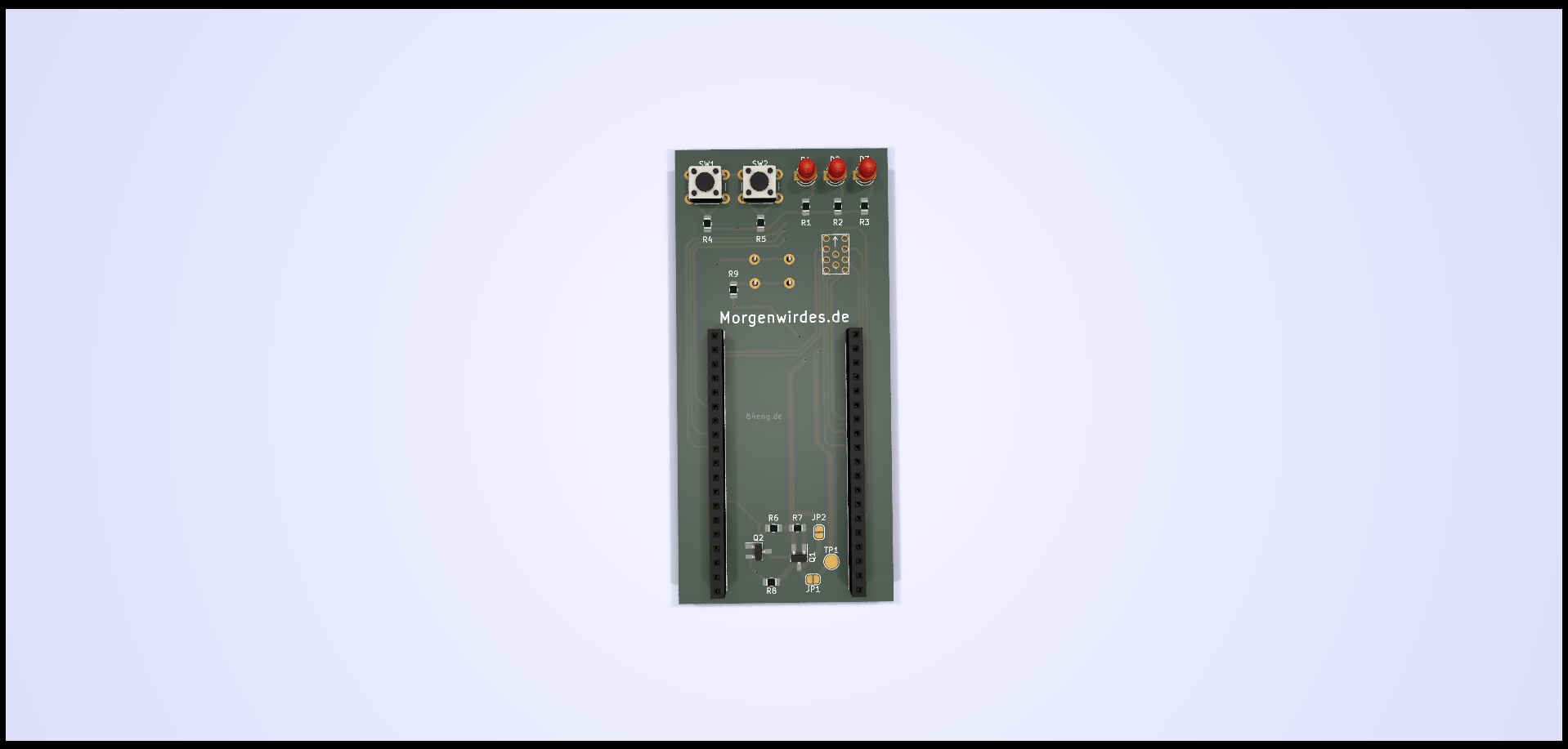
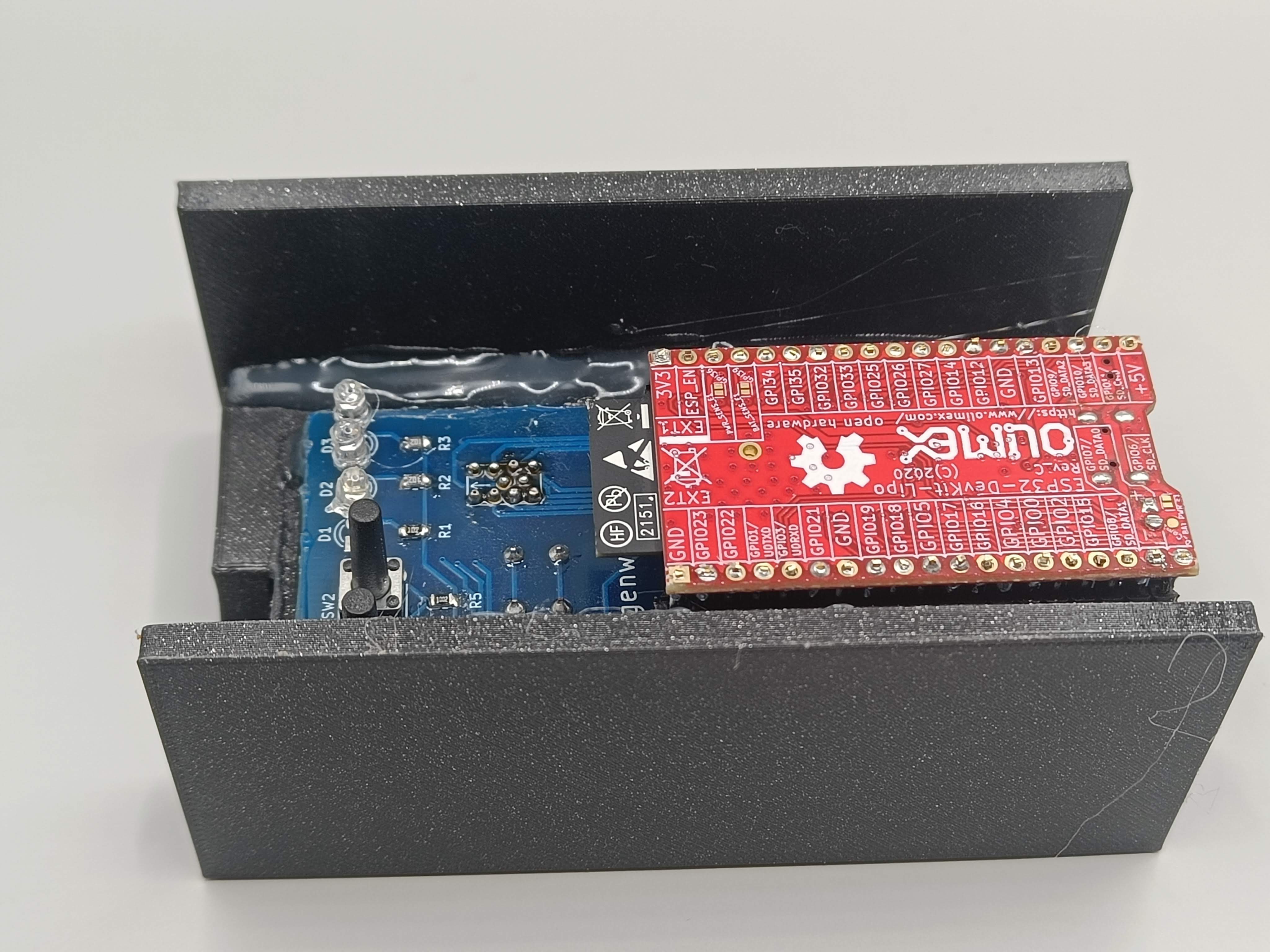
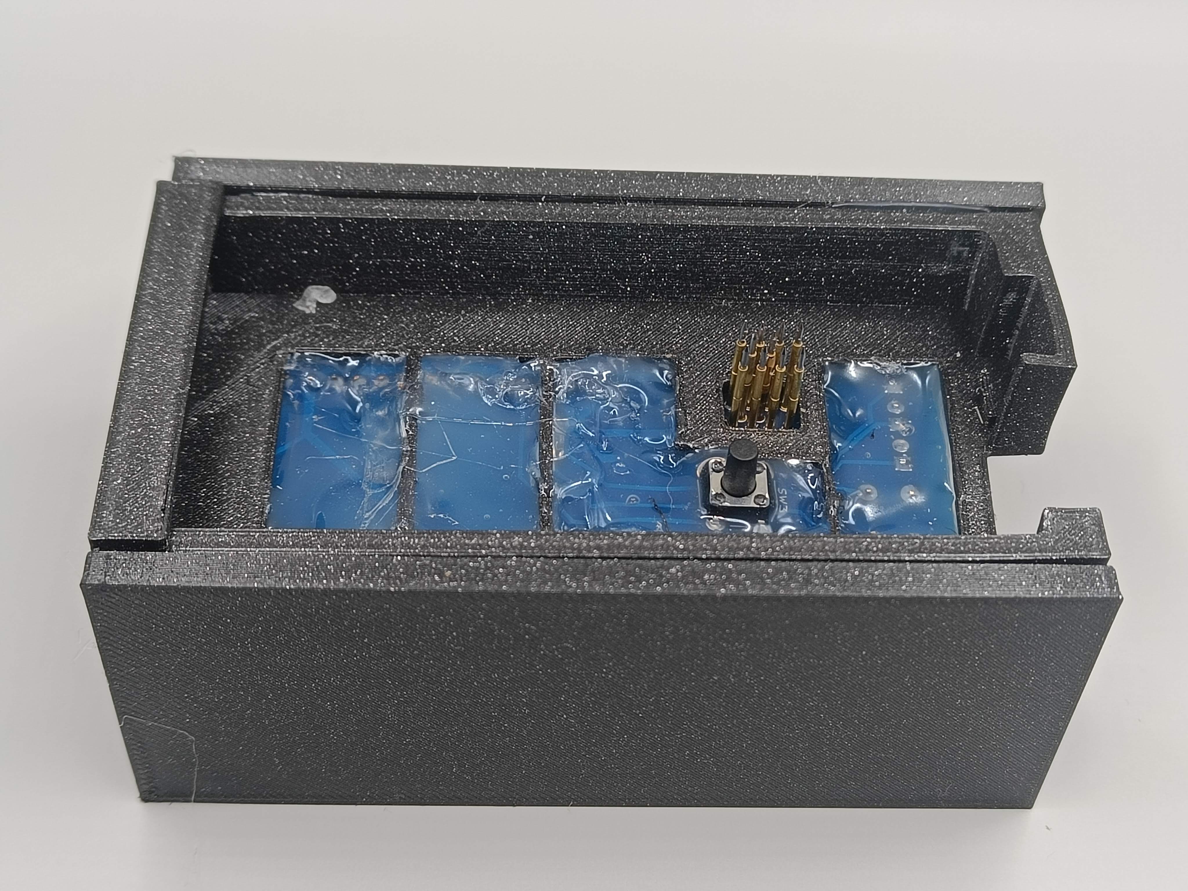
The ESP32 board needs to be solder upside down
You can order the boards from your favorite boardhouse, using the zip file in this repository.
There is no guarantee or warranty whatsoever, nor is there any promise or insinuation that this board fill fullfill any particular purpose. This board may very well not work for you, set your hair and/or, but not limited to, pants on fire, incite violance or persuade other countries to invade your country. You're on your own, chief!
| Qty | Value | Footprint | References |
|---|---|---|---|
| 6 | 10k | Resistor_SMD:R_0805_2012Metric_Pad1.20x1.40mm_HandSolder | R4, R5, R6, R7, R8, R9 |
| 3 | 1k | Resistor_SMD:R_0805_2012Metric_Pad1.20x1.40mm_HandSolder | R1, R2, R3 |
| 3 | SW_Push | Button_Switch_THT:SW_PUSH_6mm | SW1, SW2, SW3 |
| 1 | ESL-connector | esl:SOLUM_ZBS_DEBUG | U1 |
| 1 | ESP32_Devkit_JL | Connector_PinSocket_2.54mm:PinSocket_1x19_P2.54mm_Vertical | J1 |
| 1 | ESP32_Devkit_JR | Connector_PinSocket_2.54mm:PinSocket_1x19_P2.54mm_Vertical | J2 |
| 1 | G | LED_THT:LED_D3.0mm | D3 |
| 1 | Q_NMOS_GSD | Package_TO_SOT_SMD:SOT-23_Handsoldering | Q2 |
| 1 | Q_PMOS_GDS | Package_TO_SOT_SMD:SOT-23_Handsoldering | Q1 |
| 1 | R | LED_THT:LED_D3.0mm | D1 |
| 1 | SolderJumper_2_Bridged | Jumper:SolderJumper-2_P1.3mm_Bridged2Bar_RoundedPad1.0x1.5mm | JP1 |
| 1 | SolderJumper_2_Open | Jumper:SolderJumper-2_P1.3mm_Open_RoundedPad1.0x1.5mm | JP2 |
| 1 | TestPoint | TestPoint:TestPoint_Pad_D2.5mm | TP1 |
| 1 | Y | LED_THT:LED_D3.0mm | D2 |
It measures 40 × 85 mm and has 2 copper layers, 1.6 mm thick.
23 parts. The full list of its parts is on this page, with links to each part's symbol and footprint where PCBKit's library has them.
From the OpenEPaperLink/Hardware repository on GitHub, at the commit this page was made from: the board is 2.9 Flasher by Jonas/jig2.kicad_pcb and its schematic 2.9 Flasher by Jonas/jig2.kicad_sch. PCBKit opens the board in the browser, with nothing to install.
Its repository states no licence, so its author keeps all rights: ask OpenEPaperLink before reusing the design.


google/mozc-devices
Circuit diagrams and firmware source code for Gboard DIY keyboards


Duet3D/Duet-2-Hardware
The KiCAD source for the Duet 3d printer controller see www.duet3d.com