
4 layers41.3 × 19 mm
 notaroomba/keybytes444
A truly modular keyboard
Keybit is an open-source printed circuit board by notaroomba, from the notaroomba/keybytes repository on GitHub. It is a 2-layer board of 19 × 19 mm with 23 parts on 20 nets, routed with 118 tracks and 63 vias.
It is built around the YZ13515055F-02025-02. Its parts include 9 ICs, 8 resistors, 1 capacitor and 1 switch. It belongs with the keyboards and input boards and the RISC-V boards of this library.


Key Features • Video Demo • Connecting Keybits • PCB • Case • Credits • License
https://github.com/user-attachments/assets/19bec26d-6e01-4ee0-906e-7e69bace2f9c
Typing over USB:
https://github.com/user-attachments/assets/b6abd347-b68b-40f1-8e2d-c50744b8104e
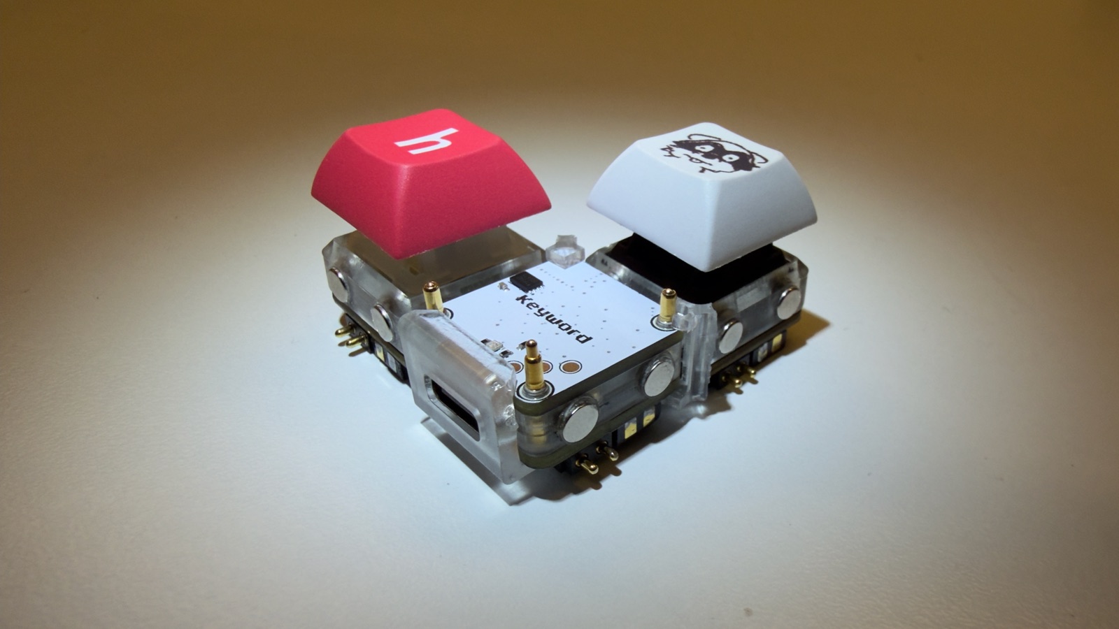
Going around a keybit, the pogo pins on the N and W sides are 3.3V, SDA, GND, SCL and on the E and S sides they are SCL, GND, SDA, 3.3V. So two keybits only work together when an N or W side touches an E or S side, which gives every joint two ways a keybit can be turned and still work: the usual way, or a quarter turn so the other matching side faces its neighbour. The left and top of the keyword take an E or S side and the right takes an N or W side.
If every keybit is the same way round any shape works, like a square with the keyword in one corner. A keybit turned the wrong way gets 3.3V on its SCL and GND on its SDA, so it gets no power and nothing behind it shows up until it's turned.
Status LED:
Updating keybits: the keyword carries the keybit firmware. After updating the keyword, put every keybit on the programming pins once and wait for green. Keybits on different firmware versions don't talk to each other, so do all of them.
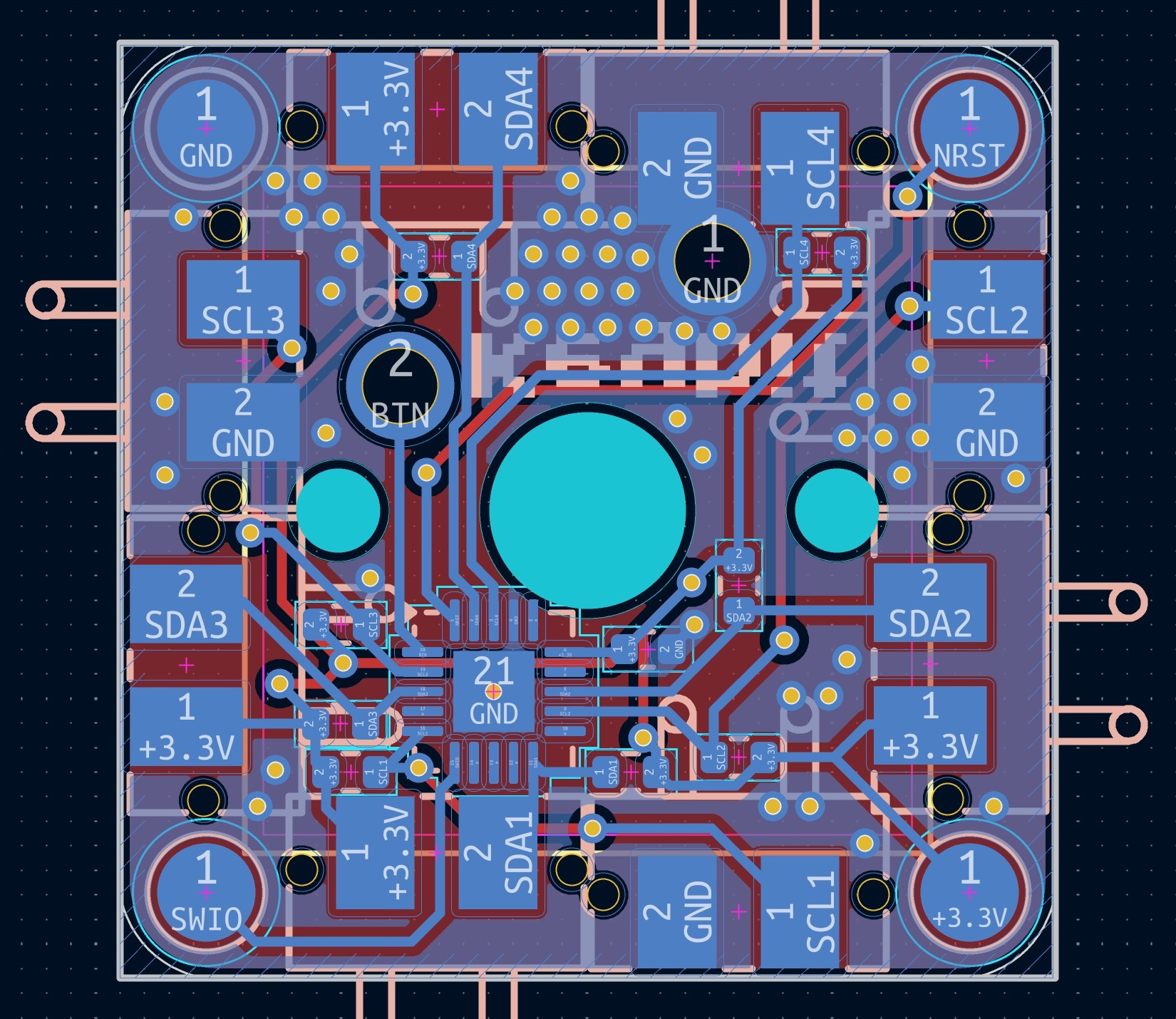
Designed in KiCad! There are two boards, the Keybit and the Keyword, and both are 1u (19.05mm x 19.05mm).
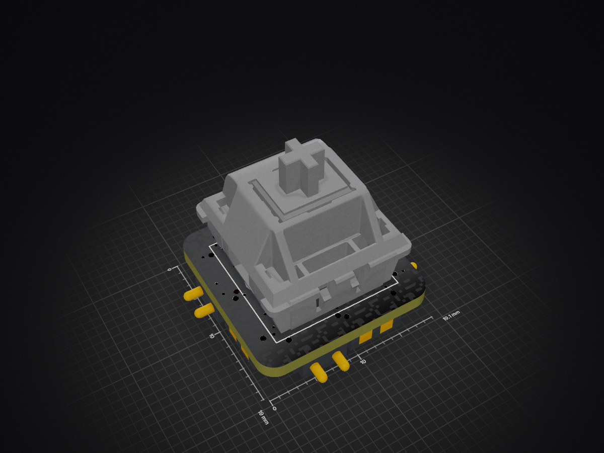
A single key with a Cherry MX switch and a CH32V003. Every side has pogo pins for 3.3V, GND and I2C so it can connect to the keyword or to other keybits, and the pads on the corners are for programming.
Schematic:
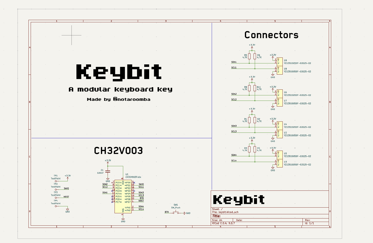
Layout:
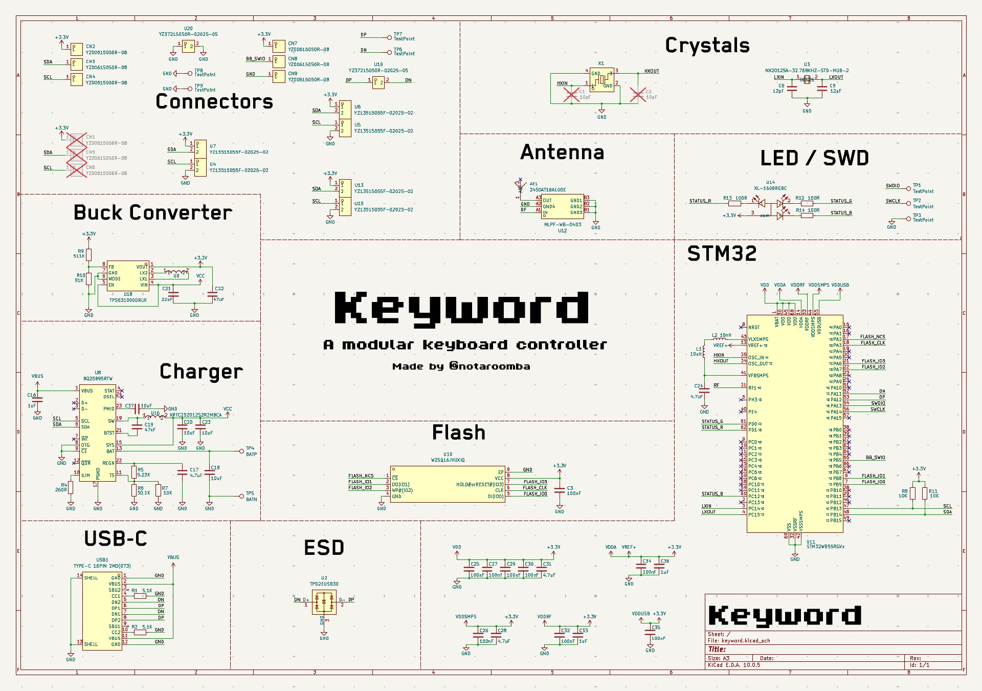
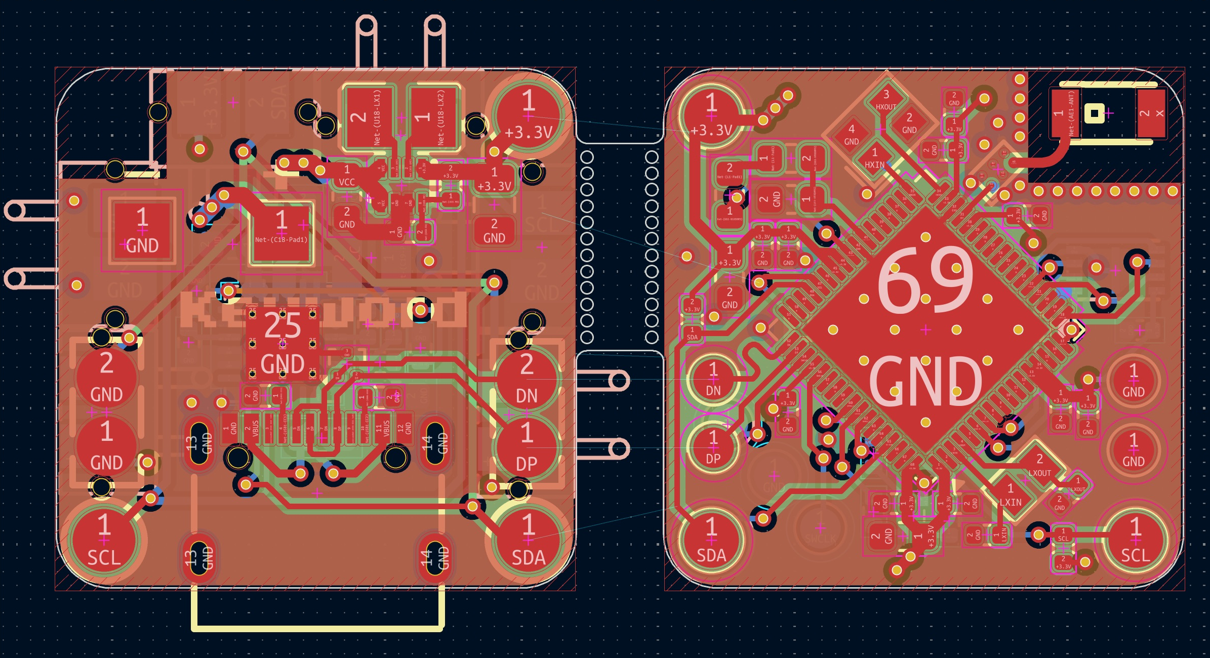
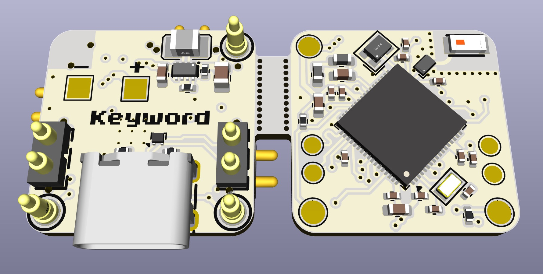
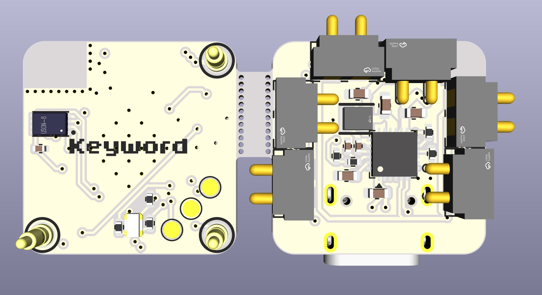
The main board that the keybits connect to. It is split into two PCBs that stack on top of each other. The top one has the STM32WB55RGV6, the antenna and the flash, and the bottom one has the USB-C, the charger and the buck-boost converter. The 3 pogo pins on the top are for programming the keybits.
Schematic:
Layout:
3D View:
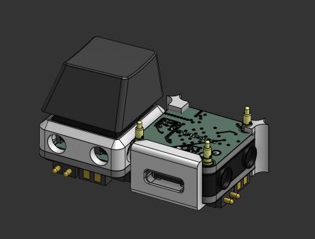
Custom designed cases in Onshape, the STEP files are in the cad folder.
This project uses:
MIT
notaroomba.dev · GitHub @NotARoomba ·
| Qty | Value | Footprint | References |
|---|---|---|---|
| 8 | 10K | Resistor_SMD:R_0402_1005Metric | R1, R2, R3, R4, R5, R6, R8, R11 |
| 8 | YZ13515055F-02025-02 | lcsc:CONN-SMD_YZ13515055F-02025-02 | U2, U3, U4, U5, U6, U7, U8, U9 |
| 4 | TestPoint | TestPoint:TestPoint_Pad_D2.0mm | TP1, TP2, TP3, TP4 |
| 1 | 100nF | Capacitor_SMD:C_0402_1005Metric | C1 |
| 1 | CH32V003FxUx | Package_DFN_QFN:QFN-20-1EP_3x3mm_P0.4mm_EP1.65x1.65mm | U1 |
| 1 | SW_Push | Button_Switch_Keyboard:SW_Cherry_MX_1.00u_PCB | SW1 |
It measures 19 × 19 mm and has 2 copper layers, 1.6 mm thick.
23 parts, built around the YZ13515055F-02025-02. The full list of its parts is on this page, with links to each part's symbol and footprint where PCBKit's library has them.
From the notaroomba/keybytes repository on GitHub, at the commit this page was made from: the board is hardware/keybit/keybit.kicad_pcb and its schematic hardware/keybit/keybit.kicad_sch. PCBKit opens the board in the browser, with nothing to install.
Its repository states no licence, so its author keeps all rights: ask notaroomba before reusing the design.


google/mozc-devices
Circuit diagrams and firmware source code for Gboard DIY keyboards


Duet3D/Duet-2-Hardware
The KiCAD source for the Duet 3d printer controller see www.duet3d.com

CRImier/MyKiCad
My KiCad boards. Can't be bothered uploading individually anymore, so here you go.