2 layers28.3 × 39.8 mm
LevelShifter
gusmanb/logicanalyzer
24 channel, 100Msps logic analyzer hardware and software
21 parts5.1kGPL-3.0

 OneForFreedom/Adibs-HackPad
My HackPad!
Adibs HackPad is an open-source printed circuit board by OneForFreedom, from the OneForFreedom/Adibs-HackPad repository on GitHub. It is a 2-layer board of 91 × 84.9 mm with 21 parts on 24 nets, routed with 106 tracks and 7 vias.
Its parts include 10 switches, 9 diodes and 1 IC. It belongs with the RP2040 boards of this library.
(Before you critisise anything, its my first time - juuustttt.. keep that in mind please lol.) I took 30 or more hours on this, trust me. I did this over the course of a week. started doing the tutorial 1:1, then I realised that you wern't meant to follow it. so I salvaged what was useable, and completely pissed my parents by spending 6pm to 12am just doing it after school over the course of the previous week. last thursday (26/06/25 dd/mm/yy) I messed up by saving old versons of my PCB files, which ruined the project. so I had to redo it. Luckily I had pictures of the schematic which let me redo that pretty easily, and the pcb was the hard bit, but got it in about 7 hours after realising that I had saved sketches in my CAD editor (Fusion) I went through all 5 stages of grief in 20 seconds
Btw it took me soo long because the concept of a PCB was alien to me.
Now since my sob story's done. lets get to the facts:
This is a 3x3 Key Matrix style MacoPad with a 0.91 inch I2C type oled (the highlight of the pain of my journey) and a rotary encoder for volume.
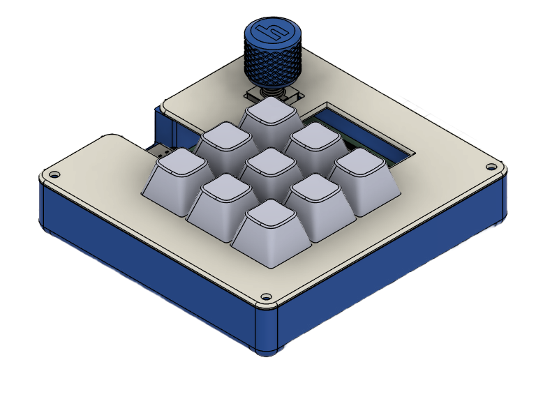
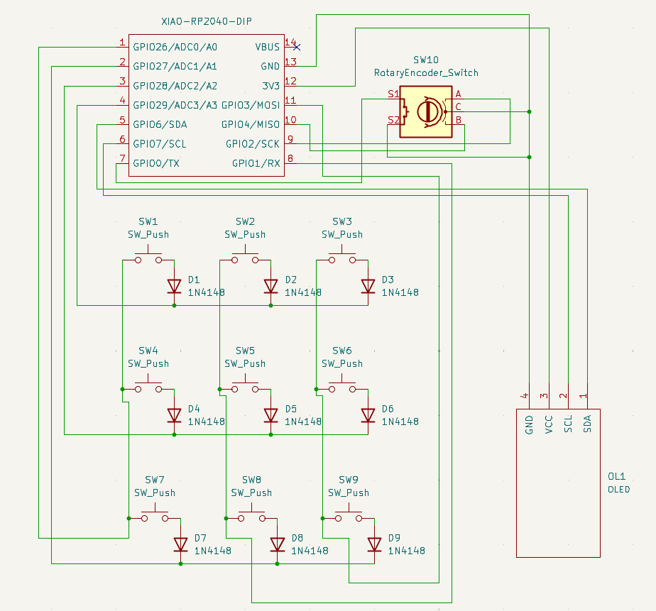
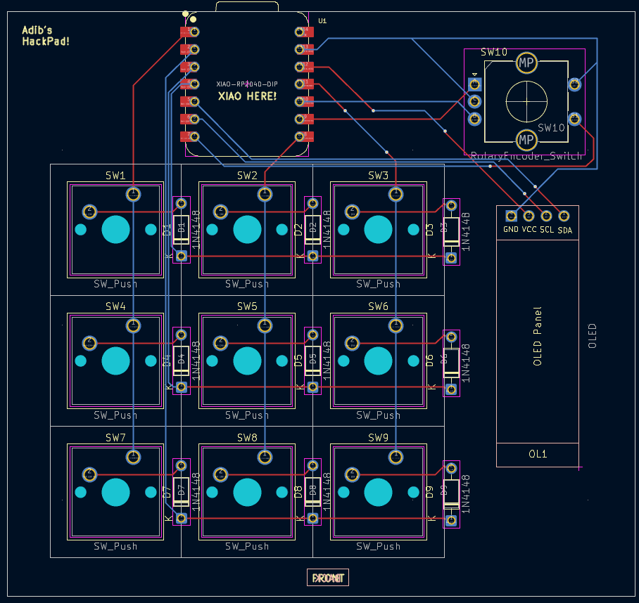
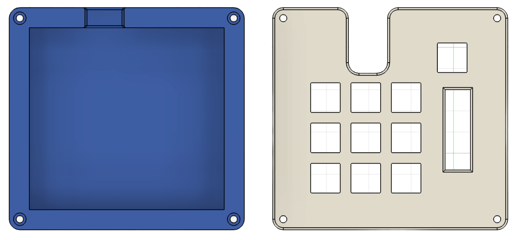
| Qty | Value | Footprint | References |
|---|---|---|---|
| 9 | 1N4148 | Diode_THT:D_DO-35_SOD27_P7.62mm_Horizontal | D1, D2, D3, D4, D5, D6, D7, D8, D9 |
| 9 | SW_Push | Button_Switch_Keyboard:SW_Cherry_MX_1.00u_PCB | SW1, SW2, SW3, SW4, SW5, SW6, SW7, SW8, SW9 |
| 1 | OLED | HP3:SSD1306-0.91-OLED-4pin-128x32 | OL1 |
| 1 | RotaryEncoder_Switch | Rotary_Encoder:RotaryEncoder_Alps_EC11E-Switch_Vertical_H20mm_CircularMountingHoles | SW10 |
| 1 | XIAO-RP2040-DIP | HP:XIAO-RP2040-DIP | U1 |
It measures 91 × 84.9 mm and has 2 copper layers, 1.6 mm thick.
21 parts. The full list of its parts is on this page, with links to each part's symbol and footprint where PCBKit's library has them.
From the OneForFreedom/Adibs-HackPad repository on GitHub, at the commit this page was made from: the board is pcb/Adib's Hackpad.kicad_pcb and its schematic pcb/Adib's Hackpad.kicad_sch. PCBKit opens the board in the browser, with nothing to install.
Its repository states no licence, so its author keeps all rights: ask OneForFreedom before reusing the design.
gusmanb/logicanalyzer
24 channel, 100Msps logic analyzer hardware and software

mntmn/amiga2000-gfxcard
MNT VA2000, an Open Source Amiga 2/3/4000 Graphics Card (Zorro II/III), written in Verilog


hackclub/OnBoard
💡 Join 1,000 teenagers and make your first PCB with a $100 grant!

drandyhaas/KiCadRoutingTools
A set of Python/Rust tools to aid routing in KiCad

Arrow-air/project-quiver
Project Quiver documentation, designs, and project artifacts.

