
2 layers95 × 95 mm
Front controls
techie66/EngineDataLogger-FrontControls
Arduino code for front controls device.
135 parts1GPL-2.0

Compact industrial mini PLC designed in KiCad
STM is an open-source printed circuit board by Noraiz963, from the Noraiz963/Mini-PLC- repository on GitHub. It is a 2-layer board of 204.5 × 113 mm with 139 parts on 197 nets, routed with 777 tracks and 61 vias.
It is built around the CH340C, SP3485CN-L and LMR14030SDDA, with the AMS1117-3.3, IRLZ44N and SS14 among its other parts. Its parts include 55 resistors, 29 diodes, 13 ICs, 10 capacitors and 9 transistors. It belongs with the STM32 boards of this library.


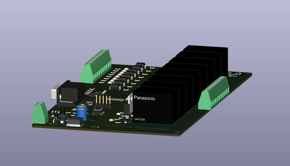
A compact industrial-style PLC board designed in KiCad, built around an STM32F407 microcontroller. It provides 8 optically isolated digital inputs, 8 relay outputs, RS-485 communication and USB-C serial/bootloader access, all powered from 24 VDC.
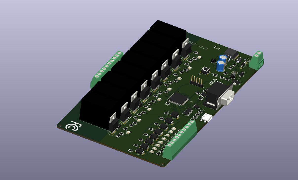
Status: Hardware design v1.0 complete. The board has not been manufactured or tested, and no firmware has been written yet.
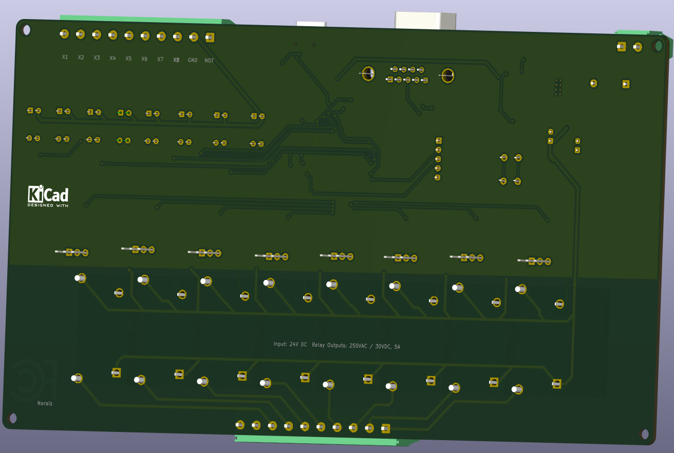
Back side showing input labels (X1 to X8), copper routing and relay output pads.
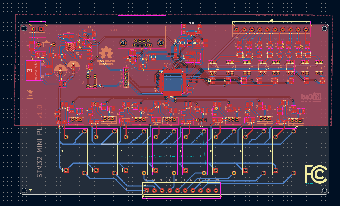
Red traces are the top copper layer and blue traces are the bottom copper layer. The logic section (power, STM32, inputs, communication) is at the top, and the relay and output section is at the bottom.
| Parameter | Value |
|---|---|
| Microcontroller | STM32F407 |
| Supply input | 24 VDC |
| Digital inputs | 8, optically isolated |
| Relay outputs | 8, rated 250 VAC / 30 VDC, 5 A (per board silkscreen) |
| Communication | RS-485 (DB9 connector), USB-C (UART bridge) |
| Programming / debug | 5-pin SWD header for ST-LINK |
| Design tool | KiCad |
| Board layers | 2 (top and bottom copper) |
| Version | v1.0 |
flowchart LR
    PWR[24 VDC input<br/>J1, F1, D1] --> BUCK[Buck converter U1]
    BUCK --> LDO[3.3 V regulator U2]
    LDO --> MCU[STM32F407<br/>U13]
    IN[Field inputs X1-X8<br/>J2] --> OPTO[Optocouplers<br/>U4-U11]
    OPTO --> MCU
    MCU --> FET[MOSFET drivers<br/>Q2-Q9]
    FET --> RLY[Relays K2-K9]
    RLY --> OUT[Outputs Y1-Y8<br/>J3]
    MCU <--> RS[RS-485 transceiver U12<br/>DB9 J4]
    MCU <--> USB[CH340C U14<br/>USB-C J19]
MCU <--> SWD[SWD header J5]| Sub-system | Key components | Description |
|---|---|---|
| Power stage | J1, F1, D1, U1, U2 | Accepts 24 VDC industrial input, protected by a fuse and a reverse-polarity diode. A switching buck converter (U1) and a 3.3 V linear regulator (U2) power the logic. |
| Processing core | U13 (STM32F407), C9 to C11 | Main microcontroller for application logic, with decoupling capacitors for stability. |
| Programming and debug | J5 (3V3, SWDIO, RST, SWCLK, GND) | 5-pin header for debugging and flashing with an external ST-LINK. Pin 1 is the 3.3 V reference (VTREF). |
| USB and serial | J19 (USB-C), U14 (CH340C) | USB-to-UART bridge for serial monitoring (printf debugging) and bootloader flashing. |
| Isolated digital inputs | J2, U4 to U11 (optocouplers) | 8 optically isolated channels that protect the STM32 from field-side voltage transients. |
| Relay output stage | K2 to K9, Q2 to Q9 (MOSFETs), D13 to D20, J3 | 8 electromechanical relays driven by MOSFET switches, with freewheeling diodes for inductive kickback protection. |
| Industrial communication | U12 (RS-485 transceiver), J4 | Differential serial interface for fieldbus networks. The hardware is suitable for Modbus RTU. |
| Ref | Function | Pins |
|---|---|---|
| J1 | 24 VDC power input | 24 V, 0 V |
| J2 | Digital inputs | X1 to X8, GND (see silkscreen) |
| J3 | Relay outputs | Y1 to Y8, plus common terminals (see silkscreen) |
| J4 | RS-485 (DB9) | Differential A/B, GND |
| J5 | SWD programming | 3V3, SWDIO, SWCLK, RST, GND |
| J19 | USB-C | UART bridge and bootloader |
Specifications above come from the design, not from measurements on a built board.
KiCad (schematic, PCB layout, 3D viewer)
Designed by: Noraiz
| Qty | Value | Footprint | References |
|---|---|---|---|
| 19 | 10K | Resistor_SMD:R_1210_3225Metric_Pad1.30x2.65mm_HandSolder | R1, R4, R19, R20, R21, R22, R23, R24, R25, R26, R41, R42, R43, R44, R45, R46 +3 |
| 16 | 4.7K | Resistor_SMD:R_1210_3225Metric_Pad1.30x2.65mm_HandSolder | R11, R12, R13, R14, R15, R16, R17, R18, R49, R50, R51, R52, R53, R54, R55, R56 |
| 16 | LED | LED_SMD:LED_1210_3225Metric_Pad1.42x2.65mm_HandSolder | D5, D6, D7, D8, D9, D10, D11, D12, D22, D23, D24, D25, D26, D27, D28, D29 |
| 8 | 10 | Resistor_SMD:R_1210_3225Metric_Pad1.30x2.65mm_HandSolder | R28, R29, R30, R31, R32, R33, R34, R35 |
| 8 | IRLZ44N | Package_TO_SOT_THT:TO-220-3_Vertical | Q2, Q3, Q4, Q5, Q6, Q7, Q8, Q9 |
| 8 | PC817 | Package_DIP:DIP-4_W7.62mm | U4, U5, U6, U7, U8, U9, U10, U11 |
| 8 | Panasonic_ALFG2PF241 | Relay_THT:Relay_SPST_Panasonic_ALFG_FormA_CircularHoles | K2, K3, K4, K5, K6, K7, K8, K9 |
| 8 | SS14 | Diode_SMD:D_SMA | D13, D14, D15, D16, D17, D18, D19, D20 |
| 4 | 100nF | Capacitor_SMD:C_0201_0603Metric_Pad0.64x0.40mm_HandSolder | C3, C4, C9, C12 |
| 2 | 100K | Resistor_SMD:R_1210_3225Metric_Pad1.30x2.65mm_HandSolder | R2, R5 |
| 2 | 10k | Resistor_SMD:R_1210_3225Metric_Pad1.30x2.65mm_HandSolder | R57, R58 |
| 2 | 1K | Resistor_SMD:R_1210_3225Metric_Pad1.30x2.65mm_HandSolder | R8, R9 |
| 2 | 2.2uf | Capacitor_SMD:C_0201_0603Metric_Pad0.64x0.40mm_HandSolder | C10, C11 |
| 2 | 22 | Resistor_SMD:R_1210_3225Metric_Pad1.30x2.65mm_HandSolder | R39, R40 |
| 2 | 47uF | Capacitor_THT:CP_Radial_D8.0mm_P2.50mm | C1, C2 |
| 2 | 5.1K | Resistor_SMD:R_1210_3225Metric_Pad1.30x2.65mm_HandSolder | R37, R38 |
| 2 | SS34 | Diode_SMD:D_SMA | D3, D21 |
| 2 | Screw_Terminal_01x10 | TerminalBlock_Phoenix:TerminalBlock_Phoenix_MKDS-1,5-10-5.08_1x10_P5.08mm_Horizontal | J2, J3 |
| 1 | 10uH | Inductor_SMD_Wurth:L_Wurth_WE-LQSH-4020 | L1 |
| 1 | 120 | Resistor_SMD:R_1210_3225Metric_Pad1.30x2.65mm_HandSolder | R10 |
| 1 | 15uF | Capacitor_SMD:C_0201_0603Metric_Pad0.64x0.40mm_HandSolder | C7 |
| 1 | 15uH | Inductor_SMD_Wurth:L_Wurth_WE-LQSH-4020 | L2 |
| 1 | 1N47xxA | Diode_THT:D_DO-41_SOD81_P10.16mm_Horizontal | D1 |
| 1 | 47uF | Capacitor_SMD:C_0201_0603Metric_Pad0.64x0.40mm_HandSolder | C5 |
| 1 | 52.3K | Resistor_SMD:R_1210_3225Metric_Pad1.30x2.65mm_HandSolder | R3 |
| 1 | AMS1117-3.3 | Package_TO_SOT_SMD:SOT-223-3_TabPin2 | U2 |
| 1 | CH340C | Package_SO:SOIC-16_3.9x9.9mm_P1.27mm | U14 |
| 1 | Conn_ARM_SWD_TagConnect_TC2030 | Connector_PinHeader_2.54mm:PinHeader_1x05_P2.54mm_Vertical | J5 |
| 1 | DE9_Pins | Connector_Dsub:DSUB-9_Pins_Horizontal_P2.77x2.84mm_EdgePinOffset9.90mm_Housed_MountingHolesOffset11.32mm | J4 |
| 1 | FQB47P06TM-AM002 | FQB47P06TM-AM002:TO-263-3_ONSEMI | Q1 |
| 1 | Fuse | Fuse:Fuse_2010_5025Metric_Pad1.52x2.65mm_HandSolder | F1 |
| 1 | LMR14030SDDA | LMR14030SDDA:VREG_LM5017MR_NOPB | U1 |
| 1 | SM712_SOT23 | Package_TO_SOT_SMD:SOT-23 | D4 |
| 1 | SMBJ36A | SMBJ36A:DIOM4336X265N | D2 |
| 1 | SP3485CN | Package_SO:SOIC-8_3.9x4.9mm_P1.27mm | U12 |
| 1 | STM32F407VGTx | Package_QFP:LQFP-100_14x14mm_P0.5mm | U13 |
| 1 | SW_Push | Button_Switch_THT:SW_PUSH_6mm | SW1 |
| 1 | Screw_Terminal_01x02 | TerminalBlock_Phoenix:TerminalBlock_Phoenix_MKDS-1,5-2-5.08_1x02_P5.08mm_Horizontal | J1 |
| 1 | USB_C_Receptacle_USB2.0_16P | Connector_USB:USB_C_Receptacle_GCT_USB4110 | J19 |
The 134 most common of 139 parts.
It measures 204.5 × 113 mm and has 2 copper layers, 1.6 mm thick.
139 parts, built around the CH340C, SP3485CN-L, LMR14030SDDA and AMS1117-3.3. The full list of its parts is on this page, with links to each part's symbol and footprint where PCBKit's library has them.
From the Noraiz963/Mini-PLC- repository on GitHub, at the commit this page was made from: the board is pcb/STM.kicad_pcb. PCBKit opens the board in the browser, with nothing to install.
Its repository states no licence, so its author keeps all rights: ask Noraiz963 before reusing the design.
techie66/EngineDataLogger-FrontControls
Arduino code for front controls device.

xmyoot/esp32-media-carrier
ESP32 multimedia carrier board with 7–24 V DC buck regulator, 3.2 W Class-D I2S audio amp, WS2812 LED ring driver, and SPI TFT display header


lcsingleton/fg2-fdim-surrogate
A carrier/backplane KiCad project that hosts four prefab modules (WeAct STM32F412RET6 Core Board, MCP2551 CAN breakout, LD24AJTA LED driver, two adjustable buck converters) and wires them into the Ford FG2 Falcon…

Oleg-mk/JLR-MOST-Reader
Listen-only MOST25 adapter for JLR: the factory stereo out over TOSLINK, the car's own volume controls applied digitally with no quality loss

Oleg-mk/MOST25-to-AUDIO
Passive MOST25 listener: Tang Nano 20K FPGA, ESP32 host, stereo I2S out with the head unit's volume, balance and tone