2 layers174 × 58 mm
Breakout 112pin Connector
rusefi/rusefi
rusefi - GPL internal combustion engine control unit
42 parts1.2k

 noma-t/navcluster
Navcluster is an open-source printed circuit board by noma-t, from the noma-t/navcluster repository on GitHub, published under the MIT licence. It is a 2-layer board of 57.2 × 123.8 mm with 42 parts on 42 nets, routed with 190 tracks and 5 vias.
Its parts include 19 switches, 18 diodes and 1 IC.
自作キーパッド。60%キーボードで失われたナビゲーションキーを補うために制作。
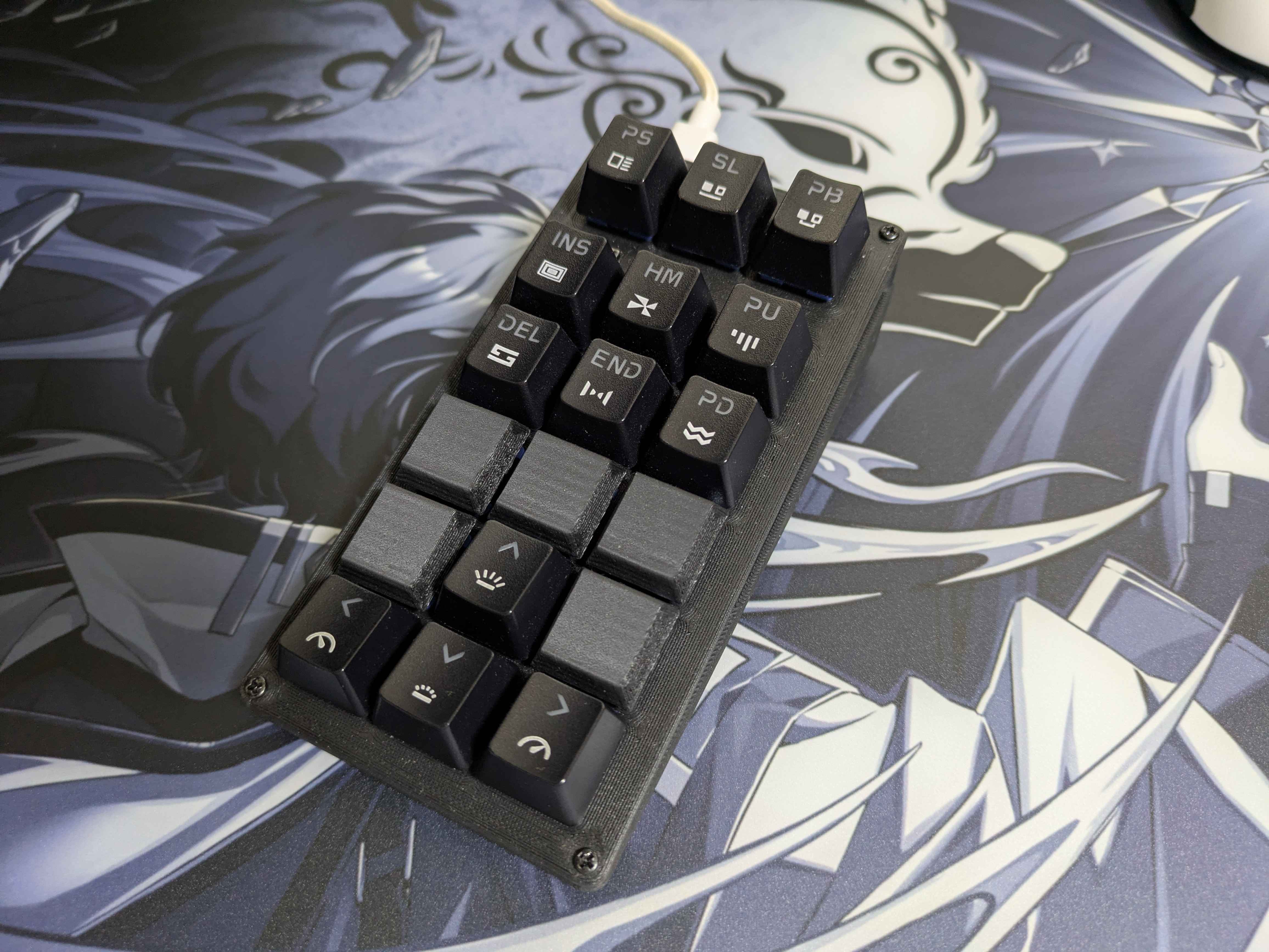
ゲーム用に60%サイズのキーボードを使用しているが、矢印キーやナビゲーションキーが存在しないため、ゲームと作業を同時進行する場面やチャット入力時に不便を感じていた。また、再生/停止・マイクミュートのような頻繁に行う操作をワンクリックで実行できる物理キーも必要としていた。
そこで、ナビゲーションキー部分をそのまま抜き出したようなキー配置のキーパッドを自作することにした。
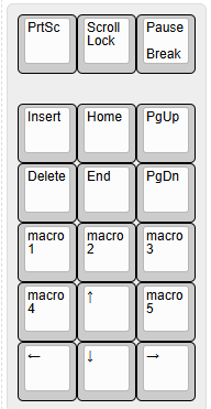
一般的なキーボードのナビゲーションキー部分をそのまま抜き出したような配置・サイズ感を意識した。既存のキーボードと近い感覚で使えるため、使用時の違和感が少ない。
通常のキーボードであれば空きスペースとなる矢印キー上の5キー分をマクロキーとして割り当て、スペースを有効活用した。
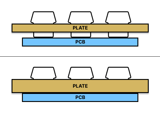
Pro Micro を基板の裏側に配置することで、マイコン部分が外側に飛び出さず、余計なスペースを取らないようにした。
マイコンを裏側に配置したことで表側に飛び出すピンへの対策として、トッププレートの設計を工夫した。トッププレートが基板と接触する構造にすることで、PLA樹脂の剛性でも問題なく機能するようにした。
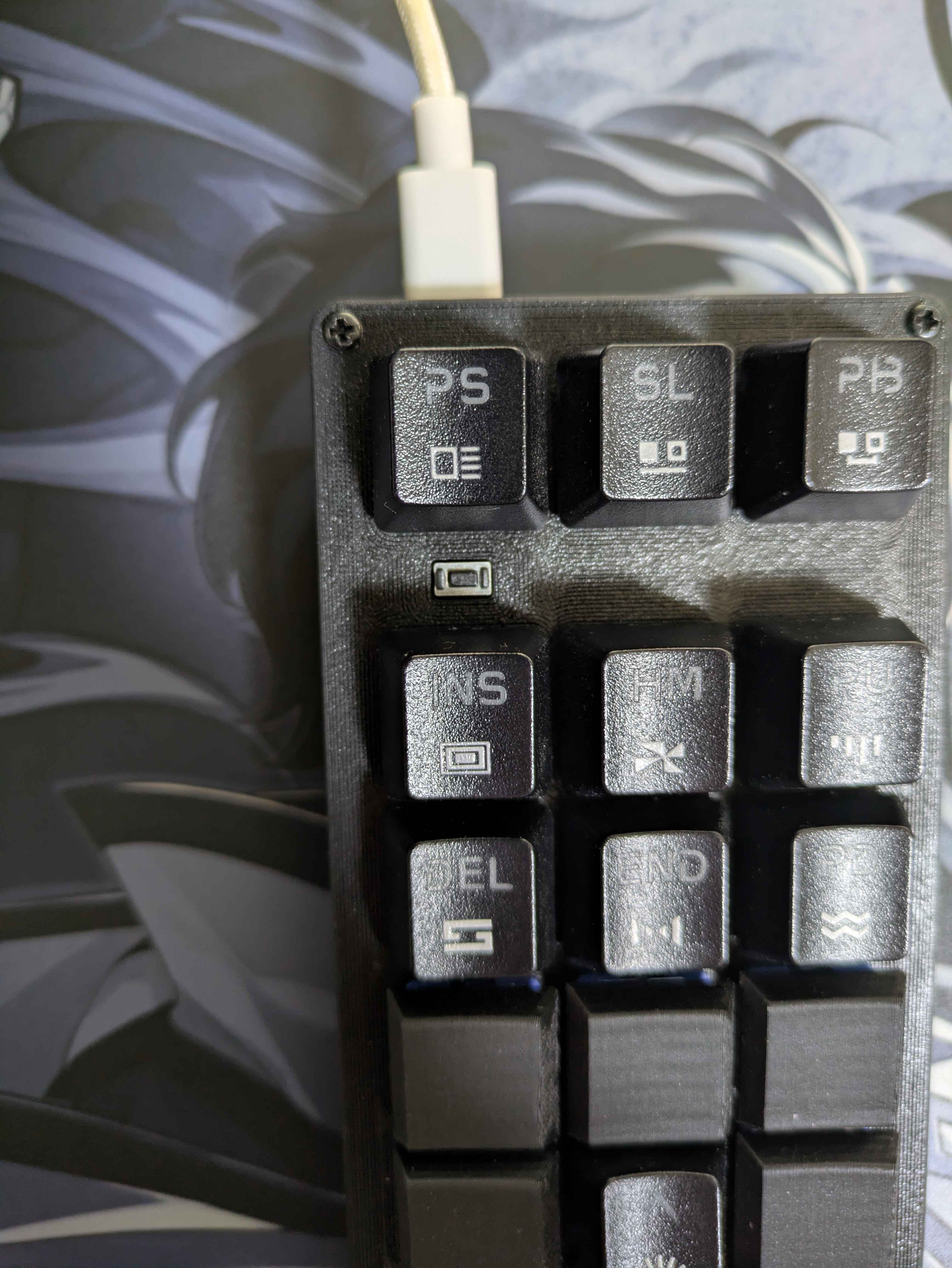
ファームウェア更新時にリセットスイッチへアクセスしやすく、かつデザインを損ねないよう、表側のナビゲーションキーとマクロキーの間に配置した。
マクロキーとナビゲーションキーでキーキャップの高さを変えることで、触覚的にキー配置を把握できるようにした。
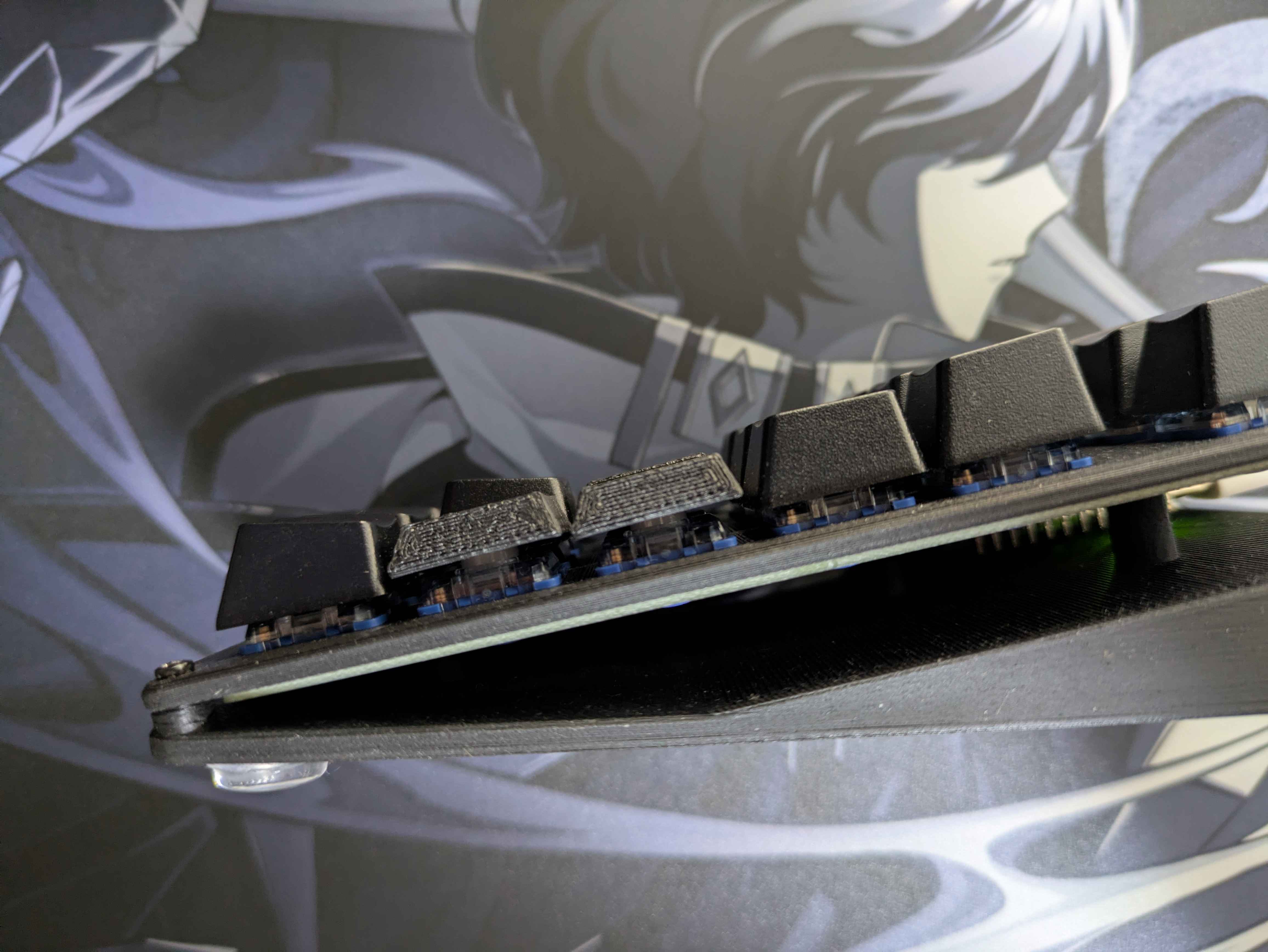
Kailh Choc V2 スイッチを使用し、薄型かつコンパクトな仕上がりにした。
| パーツ | 詳細 | リンク |
|---|---|---|
| マイコン | Pro Micro(ATmega32U4) | https://www.amazon.co.jp/dp/B0DHGTLG6W |
| キースイッチ | Kailh Choc V2 Deep Sea | https://www.amazon.co.jp/dp/B0F8NQ3WFZ |
| キーキャップ | もう使っていないキーボードから拝借+一部3Dプリンターで自作 | - |
| ダイオード | 1N4148W | https://www.amazon.co.jp/dp/B0FPCSTCLK |
| リセットスイッチ | タクトスイッチ | https://www.amazon.co.jp/dp/B008DS188Y |
| ネジ | M3 | - |
| 接続ケーブル | USB-C to A | - |
| PCB | JLCPCB 発注 | - |
| ケース | 3Dプリンターで自作 | - |
| フットプリント | リンク |
|---|---|
| kbd | https://github.com/foostan/kbd |
| random-keyboard-parts | https://github.com/ai03-2725/random-keyboard-parts.pretty |
| Keebio-Parts | https://github.com/keebio/Keebio-Parts.pretty |
navcluster/
├── firmware/
│   ├── keyboard.json          # マトリックス・ピン・レイアウト定義
│   └── keymaps/default/
│       └── keymap.c           # キーマップ・マクロ定義
├── pcb/
│   ├── navcluster.kicad_pro
│   ├── navcluster.kicad_sch   # 回路図
│   ├── navcluster.kicad_pcb   # 基板レイアウト
├── case/
│   └── navcluster-case.step         # ケース・トッププレート
├── images/
│   └── ...
└── README.md# 初回のみ
qmk setup
# firmware/ フォルダを keyboards/navcluster/ に配置後
# ビルド
qmk compile -kb navcluster -km default
# 書き込み(実行後すぐ RST-GND をショート)
qmk flash -kb navcluster -km default"features": {
"tap_dance": true,
"mousekey": true,
"extrakey": true
}| ソフトウェア | 用途 |
|---|---|
| QMK Firmware | ファームウェア |
| KiCad | 回路図・基板設計 |
| Fusion360 | ケース設計 |
| JLCPCB | PCB 発注 |
MIT License - see LICENSE
| Qty | Value | Footprint | References |
|---|---|---|---|
| 18 | D | kbd_Parts:Diode_TH_SMD | D1, D2, D3, D4, D5, D6, D7, D10, D11, D12, D13, D14, D15, D16, D17, D18 +2 |
| 18 | SW_Push | kbd_SW:Choc_v2 | SW1, SW2, SW3, SW4, SW5, SW6, SW7, SW10, SW11, SW12, SW13, SW14, SW15, SW16, SW17, SW18 +2 |
| 1 | Micon_BLEMicroPro | kbd_Parts:Micon_BMP_7sKB | U1 |
| 1 | SW_Push | kbd:ResetSW | SW19 |
The 38 most common of 42 parts.
It measures 57.2 × 123.8 mm and has 2 copper layers, 1.6 mm thick.
42 parts. The full list of its parts is on this page, with links to each part's symbol and footprint where PCBKit's library has them.
From the noma-t/navcluster repository on GitHub, at the commit this page was made from: the board is pcb/navcluster.kicad_pcb and its schematic pcb/navcluster.kicad_sch. PCBKit opens the board in the browser, with nothing to install.
Its repository publishes it under the MIT licence: you may reuse it on that licence's terms (keep the author's notice, and for a copyleft licence share your changes alike).
rusefi/rusefi
rusefi - GPL internal combustion engine control unit


hackclub/sprig
🍃 Learn to code by making games in a JavaScript web-based game editor.

jamro/tiny-engineer
A small desktop robot that brings an AI coding assistant to life, physically acting out when it reads files, thinks, writes code, and finishes work.

hoglet67/RGBtoHDMI
Bare-metal Raspberry Pi project that provides pixel-perfect sampling of Retro Computer RGB/YUV video and conversion to HDMI

hackclub/OnBoard
💡 Join 1,000 teenagers and make your first PCB with a $100 grant!

