2 layers26 × 44 mm
Compact carrier board
jamro/tiny-engineer
A small desktop robot that brings an AI coding assistant to life, physically acting out when it reads files, thinks, writes code, and finishes work.
7 parts1.1k
 jamro/tiny-engineer1.1k
A small desktop robot that brings an AI coding assistant to life, physically acting out when it reads files, thinks, writes code, and finishes work.
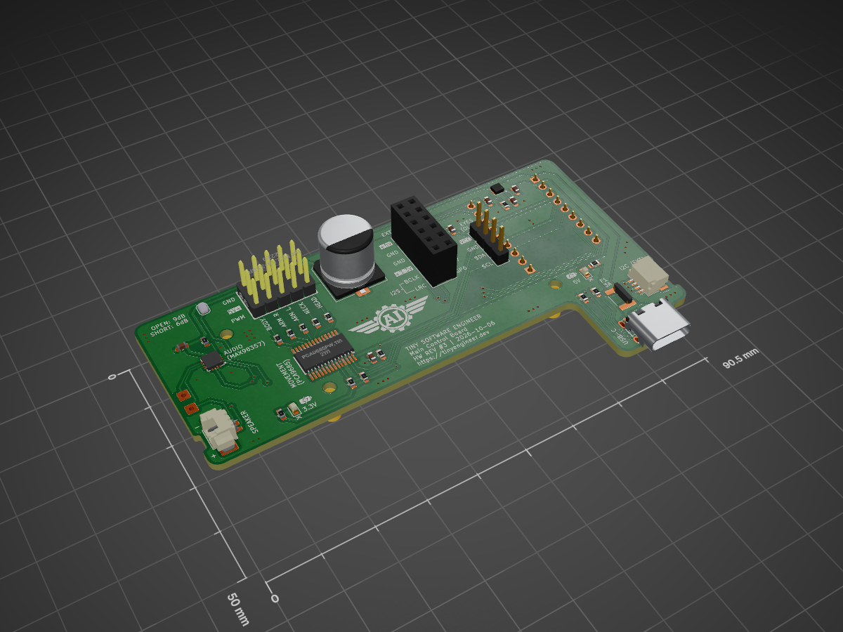
Main control board is an open-source printed circuit board by jamro, from the jamro/tiny-engineer repository on GitHub. It is a 2-layer board of 90.5 × 50 mm with 42 parts on 59 nets, routed with 340 tracks and 60 vias.
It is built around the MAX98357AETE+T, CC0603KRX7R9BB104 and PM254-1-09-Z-8.5, with the KT-0603R, JVJ16V1000M10X10 and BSMD1812-300-16V among its other parts. Its parts include 14 resistors, 7 capacitors, 6 connectors, 4 ICs and 2 diodes. It belongs with the robots and motor control boards and the ESP32 boards of this library.


Small distribution PCB that sits under the ESP32-C3-Zero where it mounts through the desk's ESP slot, fanning its I2C/I2S/power pins out to the PCA9685, OLED, MAX98357A amp, and servo power — instead of point-to-point wiring.
J_PWR (5V/GND + external USB
D+/D-), J_SERVO, J_I2C_OLED, J_I2C_PCA, J_I2Sservos.json) — the SG90 and FS0307 presets
produce different desk dimensions per the parametric design docs, and this
board's fit has not been verified against either of them. Re-check the
ESP slot dimensions in your own exported desk model before relying on this
outline if you're on a different preset. See docs/hardware/interfaces.md
for the canonical net map (5V/3.3V domains, GP0-GP4 assignments); this
board implements that map in copper.carrier-fab-v3-replacement_Y5 upload was produced and
shipped by JLCPCB (not yet received). That batch carries the mirrored
socket map this revision fixes — see "Mirrored socket map (boards in
transit)" below for the assembly workaround. Its drilling is fine: the Y5
drill export is a single 0.9mm tool over all 37 holes and JLC's own CAM
layer a single aperture, so the 7-undersized-hole defect of the earlier
_Y3 upload never reached a physical board.compact-carrier-board.kicad_pcb — KiCad 10 board sourcecompact-carrier-board.kicad_pro — KiCad 10 project file (no .kicad_sch
— this board has no schematic, laid out directly from footprints)carrier-board-render.png — 3D top render, regenerated with
kicad-cli pcb render --side top after the row swap and silk additionsGerbers, drill, BOM, and CPL are generated outputs, not source — regenerate
them from compact-carrier-board.kicad_pcb when ordering rather than
relying on a committed copy. J_ESP1/J_ESP2 carry real Value/LCSC
fields and each footprint has a real origin at its own center, so
kicad-cli pcb export pos produces correct positions directly (verified:
(13.00, -16.89) / (13.00, -1.65)) — no manual patching. J_PWR,
J_SERVO, J_I2C_OLED, J_I2C_PCA, and J_I2S are flagged
exclude_from_bom/exclude_from_pos_files so they never appear in either
export. There's no .kicad_sch, so kicad-cli has no BOM-export
subcommand for this board (that's a schematic-only feature) — a BOM script
or fab-tool plugin reading the .kicad_pcb's footprint properties directly
now gets correct Value/LCSC without hand-derivation.
J_PWR, J_SERVO, J_I2C_OLED, J_I2C_PCA, and J_I2S are bare
through-holes for direct wire connections, not connector footprints to
populate — excluded from BOM/CPL at the footprint level (see above).
J_ESP1/J_ESP2 are the one real part: Kinghelm KH-2.54FH-1X9P-H3.5
(LCSC/JLCPCB C55778388), a 2.54mm 1×9 THT female header. There's no 2×9 part
— the
ESP32-C3-Zero's socket needs two of these strips, one per row. The board
models this as two separate footprint objects, J_ESP1 (the inner row,
nearer the wire end: 5V/GND/3V3/GPIO0-5) and J_ESP2 (the outer row,
nearest the slot edge: GPIO21-GPIO6), each a real
9-pad object with its own designator — not one 2×9 footprint with a
quantity hint in prose. JLCPCB's assembly tooling (and most BOM tooling)
determines quantity by counting designators, not by parsing Comment text, so
a generated BOM lists both on one row as "J_ESP1,J_ESP2" (identical part,
JLC's own convention for grouping identical components) — that reads as qty
2 unambiguously.
A generated CPL has one row per designator, J_ESP1 and J_ESP2, each at
its own row's real center — (13.00, 16.89) and (13.00, 1.65) in the board's
own coordinates — read directly by kicad-cli pcb export pos from each
footprint's own origin, no hand-derivation needed.
Measured directly from an exported desk part (not estimated): the ESP mounting slot is 25.0 × 18.5mm, and three of its four sides sit only 3.0–3.6mm from full-height enclosure walls — too tight for any connector housing. Only the front is open. That forced the layout:
J_PWR (now 4-pin — 5V/GND plus the external USB D+/D-, see
below), J_SERVO (5V direct to PCA9685 V+, bypassing the ESP's own 3.3V
regulator), J_I2C_OLED, J_I2C_PCA (separate connectors, bus shared via
on-board copper — no external splitter cable), J_I2S (own on-board 5V
feed for the amp).Row placement is the part that is easy to get backwards, so name the rule: the pad map, seen from the face the module plugs into, has to be the module's component-side view. A pin-side view is the correct drawing only for a socket on the opposite face — that inversion is exactly what went wrong in the shipped batch (below).
Hold the C3-Zero component side up with its USB-C over this board's 5V-bus edge (the long edge the 5V trace hugs). Then:
J_ESP2, nearest the slot edge (y=14.15):
GPIO21, GPIO20, GPIO19, GPIO18, GPIO10, GPIO9, GPIO8, GPIO7, GPIO6.
Mechanical/no-net support except GP19 and GP18, the native USB pair —
see USB below.J_ESP1, nearer the wire end (y=29.39):
5V, GND, 3V3, GPIO0(SDA), GPIO1(SCL), GPIO2(BCLK), GPIO3(LRCLK), GPIO4(DIN), GPIO5Pins 1 and 18 land at the 5V-bus edge in both rows, and that is what fixes the module's USB-C to that edge. Traversing 1 to 18 reads counter-clockwise from above, matching Waveshare's own pinout art (1-9 down the left column, 10-18 up the right, USB-C at the top).
Per docs/hardware/interfaces.md: the robot's single external USB-C (Adafruit
5993) carries both power and the ESP32's native USB D+/D- lines, so flashing
and serial CDC work through the panel-mount jack once the desk is sealed —
the C3-Zero's own onboard USB-C is left unused. No ESD or series-resistor
circuitry is specified for this link; it's a direct connection.
J_PWR pin | Net | Goes to |
|---|---|---|
| 1 | GND | common ground |
| 2 | D+ | ESP32 GPIO19 (outer-row pad, native USB DP) |
| 3 | D− | ESP32 GPIO18 (outer-row pad, native USB DM) |
| 4 | 5V | ESP32 5V rail, PCA9685 V+ (via J_SERVO), MAX98357A |
D+/D- run down the same 2.54mm grid columns as their own pads (x=20.42 and
22.96), which sits half a pitch off J_I2C_OLED/J_I2C_PCA's grid, so they
never cross those connectors' pads on the way past. Since the row swap they
also pass the inner row, where the 3V3 and SDA holes occupy those two
columns, so each line takes one short lateral jog into the adjacent lane
(1.27mm off-axis, 0.42mm to the nearest pad edge) and returns — still F.Cu,
no vias. Each line measures 36.088mm and the two are exactly length-matched;
that is 16mm longer than before the swap, which is electrically unremarkable
at full-speed 12 Mbps.
The shipped boards (carrier-fab-v3-replacement_Y5) have the two socket
rows the wrong way round. Their pad map is the C3-Zero seen from its pin
side, which is the correct drawing only for a socket on the opposite face;
as fabricated, a component-side-up module does not mate.
Caught by handedness, which no rotation can change: on the module
(component side, USB-C up) pins 1-9 run DOWN the left column and 10-18 UP
the right, so 1 to 18 is counter-clockwise; on those boards J_ESP1 1 to 9
runs left-to-right along the outer row and J_ESP2 10 to 18 right-to-left
along the inner row, i.e. clockwise.
This revision fixes the source — rows swapped in copper, nothing moved mechanically. For the boards in transit, fix it at assembly: solder both female strips to the pour face (B.Cu) and run that face up. From the pour face you see the mirror of the F.Cu artwork, which is the component-side map, so the module mates. What that build costs: the module's own USB-C ends up over the long edge facing the opposite wall from this revision's intent (unused either way — the Adafruit 5993 jack carries power and CDC), the silkscreen ends up underneath so mark pin 1 before assembly, and the wire-end connector positions mirror left-right, so the runs to the PCA9685 / OLED / amp swap sides.
kicad-cli pcb drc --severity-all (KiCad 10.0.6, run without
--refill-zones so it judges the on-disk fill) reports 0 violations and
0 unconnected items — and that statement now means something. The
project's DRC floors used to be min_clearance 0.0, min_silk_clearance
0.0, min_text_height 0.8 and min_text_thickness 0.08, so DRC could not
have failed on clearance, silk overlap or undersized text however bad they
got. They are now 0.2 / 0.15 / 1.0 / 0.15, matching JLCPCB's floors and
its standard-font minimum. Schematic parity is not checked and cannot be —
there is no .kicad_sch for this board, and --schematic-parity answers
"Schematic parity tests require a fully annotated schematic".GP21-GP6 (outer) and 5V, GND, 3V3, GP0-GP5 (inner) with a USB
arrow pointing at the 5V-bus edge; each wire-end connector carries its own
pin names (3V3/SDA/SCL/GND on both I2C headers, 5V/BCLK/LRC/DIN/GND on
J_I2S, GND/D+/D-/5V on J_PWR, 5V/GND on J_SERVO). 48 silk items,
all 1.0mm height / 0.15mm stroke. Placement is checked geometrically, not
by DRC — 0 silk-to-silk overlaps, 0.421mm minimum silk-to-pad, 0.383mm
minimum silk-to-edge. Before this the board carried nothing but seven
reference designators, which is why a mirrored pad map was invisible both
in the render and on the bare board.min_text_thickness was 0.08. All seven are now 1.0mm / 0.15mm.
J_I2C_PCA, J_PWR and J_SERVO moved to clear the new pin-name bands,
and every label is re-checked against the 0.30mm edge margin — three of
them sit at exactly that margin, so the larger text boxes were nudged back
inside rather than allowed to overhang.J_ESP1, J_ESP2, J_I2C_OLED, J_I2C_PCA)
were printing 0.2–0.6mm past the board's left edge — visually confirmed,
not just a DRC technicality. Each footprint's own text bounding box (not
an estimate) was used to shift the label right just enough to sit at a
0.3mm margin from the edge; the render below reflects the fix.J_ESP1
pin 2, GND) close enough to the zone's own boundary that a fresh zone
refill could fail to route a thermal-relief connection to them, especially
after the J_ESP2 drill fix changed nearby pad geometry. Swept the inset
from 1.0mm down to 0.3mm in 8 steps against the drill-fixed board, each
with a fresh kicad-cli pcb drc --refill-zones: 1.0mm and 0.8mm both
reproducibly fail with 1 unconnected pad; every value from 0.6mm down to
0.3mm passes with 0. 0.5mm sits in the middle of that verified-safe range
— well clear of the failure boundary and with real margin above JLCPCB's
~0.2–0.3mm copper-to-edge floor.pcbnew.ZONE_FILLER Python API) and re-verified with kicad-cli pcb drc
run without --refill-zones — that flag only recomputes the fill
in-memory for the check, it does not persist to the file, so a stale
on-disk fill can pass DRC while still being wrong in the Gerbers. This bit
us once already in this revision's history.| Qty | Value | Footprint | References |
|---|---|---|---|
| 6 | 100nF | Capacitor_SMD:C_0603_1608Metric | C1, C3, C4, C5, C6, C7 |
| 5 | 220 | Resistor_SMD:R_0603_1608Metric | R6, R7, R8, R9, R10 |
| 3 | MountingHole | MountingHole:MountingHole_2.2mm_M2 | H1, H2, H3 |
| 2 | 1k | Resistor_SMD:R_0603_1608Metric | R13, R14 |
| 2 | 4.7k | Resistor_SMD:R_0603_1608Metric | R4, R5 |
| 2 | 5.1k | Resistor_SMD:R_0603_1608Metric | R1, R2 |
| 2 | Conn_ESP32 | Connector_PinSocket_2.54mm:PinSocket_1x09_P2.54mm_Vertical | J7, J8 |
| 2 | LED | LED_SMD:LED_0603_1608Metric | D1, D2 |
| 2 | TestPoint | Connector_Wire:SolderWire-0.25sqmm_1x01_D0.65mm_OD2mm | TP1, TP2 |
| 1 | 1000uF | Capacitor_SMD:CP_Elec_10x10.5 | C2 |
| 1 | 10k | Resistor_SMD:R_0603_1608Metric | R3 |
| 1 | 1M | Resistor_SMD:R_0603_1608Metric | R12 |
| 1 | 2.2k | Resistor_SMD:R_0603_1608Metric | R11 |
| 1 | 3A PPTC | Fuse:Fuse_1812_4532Metric | F1 |
| 1 | Conn_01x02_Pin_Speaker | Connector_Molex:Molex_PicoBlade_53261-0271_1x02-1MP_P1.25mm_Horizontal | J1 |
| 1 | Conn_02x06_Odd_Even | Connector_PinHeader_2.54mm:PinHeader_2x06_P2.54mm_Vertical | J4 |
| 1 | Conn_OLED | Connector_PinHeader_2.54mm:PinHeader_1x04_P2.54mm_Vertical | J2 |
| 1 | Conn_extension | Connector_JST:JST_SH_SM04B-SRSS-TB_1x04-1MP_P1.00mm_Horizontal | J3 |
| 1 | HX PZ2.54-3X5P ZZ | easyeda:HDR-TH_15P-P2.54-V-M-R3-C5-S7.5 | U2 |
| 1 | MAX98357AETE+T | easyeda:TQFN-16_L3.0-W3.0-P0.50-BL-EP1.5 | U3 |
| 1 | NetTie_2 | NetTie:NetTie-2_SMD_Pad2.0mm | NT1 |
| 1 | PCA9685PW,118 | easyeda:TSSOP-28_L9.7-W4.4-P0.65-LS6.4-TL | U1 |
| 1 | SolderJumper_gain_6dB_limit | Jumper:SolderJumper-2_P1.3mm_Bridged_RoundedPad1.0x1.5mm | JP1 |
| 1 | TPS259571DSGR | easyeda:WSON-8_L2.0-W2.0-P0.50-TL-EP | U4 |
| 1 | TYPE-C 16PIN 2MD | easyeda:USB-C-SMD_TYPE-C-16PIN-2MD-073 | USB1 |
It measures 90.5 × 50 mm and has 2 copper layers, 1.6 mm thick.
42 parts, built around the MAX98357AETE+T, CC0603KRX7R9BB104, PM254-1-09-Z-8.5 and KT-0603R. The full list of its parts is on this page, with links to each part's symbol and footprint where PCBKit's library has them.
From the jamro/tiny-engineer repository on GitHub, at the commit this page was made from: the board is hardware/boards/main-control-board/main-control-board.kicad_pcb and its schematic hardware/boards/main-control-board-servo-tester/main-control-board-servo-tester.kicad_sch. PCBKit opens the board in the browser, with nothing to install.
Its repository states no licence, so its author keeps all rights: ask jamro before reusing the design.
jamro/tiny-engineer
A small desktop robot that brings an AI coding assistant to life, physically acting out when it reads files, thinks, writes code, and finishes work.

jamro/tiny-engineer
A small desktop robot that brings an AI coding assistant to life, physically acting out when it reads files, thinks, writes code, and finishes work.

enkhbold470/kicad-projects
Five KiCad 10 boards (4- and 6-layer): ESP32-S3 industrial gateway, USB-C PD bench supply, RP2040 logic analyzer, FOC motor controller, iCE40 FPGA board.

enkhbold470/pd-brick
USB-C Power Delivery bench supply: STUSB4500 sink, LM5176 buck-boost, INA228 monitor, 1.2-22 V set over I2C by an ESP32-S3. 4-layer KiCad 10 board.

tomrodinger/servomotor
Open-source NEMA-17 integrated servomotor (motor + closed-loop driver + controller + encoder). RS-485, Python/Arduino libraries, MCP server for AI control. Hardware, firmware and software.

mteichtahl/trace
trace runs a repository by itself and gives Claude the tools to do electronics work in it. It is generalised from the loop that runs Potroller.

donaldbell/productspeedrun
Let's see how quickly we can get a product idea off the ground.

Mowibox/chromapi_motherboard
Raspberry Pi control HAT dedicated to the quadruped robot Chromapi.

houseofthe051010/ESP32-Walkie-Talkie-V2
This ESP32 Walkie Talkie is redesigned with a SX1262 radio, a PCB, and a full case redesign.
