2 layers60 × 30 mm
Controller
google/mozc-devices
Circuit diagrams and firmware source code for Gboard DIY keyboards
11 parts3kApache-2.0
 nicklabsx/TMP118-Sensor-Array-Module-Minitask
Compact TMP118-based I2C temperature sensor array module with custom PCB and enclosure concept.
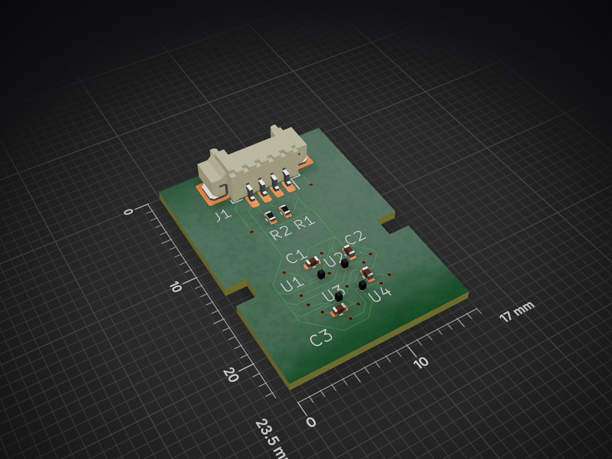
Tmp118 sensor array module is an open-source printed circuit board by nicklabsx, from the nicklabsx/TMP118-Sensor-Array-Module-Minitask repository on GitHub. It is a 2-layer board of 17 × 23.5 mm with 11 parts on 4 nets, routed with 140 tracks and 15 vias.
Its parts include 4 capacitors, 4 ICs, 2 resistors and 1 connector. It belongs with the sensors and measurement boards of this library.
Compact TMP118-based I2C temperature sensor array module with custom PCB and enclosure concept.
The repository contains the KiCad PCB project, project-local TMP118 symbol/footprint libraries, FreeCAD enclosure model, STEP exports and preview images.
hardware/kicad/        KiCad project, schematic, PCB layout and local libraries
mechanical/freecad/    FreeCAD enclosure source model
exports/step/          PCB and enclosure STEP exports
docs/images/ Preview images and screenshotsThe PCB is organized into a compact sensor area and a connector/interface area. The four TMP118 sensors are arranged as a centered 2x2 cluster, while the connector and pull-up resistors are kept outside the immediate sensor region.
A 2-layer routing approach is used to keep the dense sensor area routable while maintaining a compact layout. Local decoupling is placed close to the corresponding sensors, and the I2C lines are handled as shared bus nets.
A project-local TMP118 symbol and footprint are included to keep the KiCad project self-contained. The footprint uses the TMP118 package ball designators:
A1 = VDD
A2 = GND
B1 = SDA
B2 = SCLA Molex PicoBlade 53261-0471 4-pin horizontal SMT connector is used as the external interface for:
VDD_3V3
GND
SDA
SCL
The horizontal connector supports a low-profile module concept and is placed at the PCB edge for direct enclosure access.
The enclosure consists of a bottom housing and a separate lid. The PCB STEP model was used as the mechanical reference for component clearance, connector position and internal fitment.
The connector remains fully exposed at the front opening. Since no sealed or IP-rated housing was specified, ventilation slots are included around the sensor area to support air exposure and reduce thermal lag.
hardware/kicad/
  KiCad project, schematic, PCB layout and local TMP118 libraries

mechanical/freecad/
  FreeCAD enclosure source model

exports/step/
  PCB reference STEP
  bottom housing STEP
  lid STEP
  enclosure assembly STEP

docs/images/
PCB and enclosure preview images| Qty | Value | Footprint | References |
|---|---|---|---|
| 4 | 10nF | Capacitor_SMD:C_0402_1005Metric | C1, C2, C3, C4 |
| 4 | TMP118 | tmp118:TMP118_YMS0004A_PicoStar | U1, U2, U3, U4 |
| 2 | 4.7k | Resistor_SMD:R_0402_1005Metric | R1, R2 |
| 1 | Conn_01x04 | Connector_Molex:Molex_PicoBlade_53261-0471_1x04-1MP_P1.25mm_Horizontal | J1 |
It measures 17 × 23.5 mm and has 2 copper layers, 0.89 mm thick.
11 parts. The full list of its parts is on this page, with links to each part's symbol and footprint where PCBKit's library has them.
From the nicklabsx/TMP118-Sensor-Array-Module-Minitask repository on GitHub, at the commit this page was made from: the board is Minitask_Project/hardware/KiCad/tmp118_sensor_array_module/tmp118_sensor_array_module.kicad_pcb and its schematic Minitask_Project/hardware/KiCad/tmp118_sensor_array_module/tmp118_sensor_array_module.kicad_sch. PCBKit opens the board in the browser, with nothing to install.
Its repository states no licence, so its author keeps all rights: ask nicklabsx before reusing the design.
google/mozc-devices
Circuit diagrams and firmware source code for Gboard DIY keyboards


FrameworkComputer/ExpansionCards
Reference designs and documentation to create Expansion Cards for the Framework Laptop

hoglet67/RGBtoHDMI
Bare-metal Raspberry Pi project that provides pixel-perfect sampling of Retro Computer RGB/YUV video and conversion to HDMI

hackclub/OnBoard
💡 Join 1,000 teenagers and make your first PCB with a $100 grant!


tardate/LittleArduinoProjects
a collection of "Little Electronic & Arduino Projects", most involving electronics or an Arduino in one way or another!

basilfx/TRADFRI-Hacking
Hacking IKEA TRÅDFRI products, such as light bulbs, window blinds and other accessories.