


2 layers67.1 × 46 mm
Interposer
nherbaut/pico-power-sensor
This board sockets a Pico 2 W, provides five programmable green LEDs and a microSD slot, and connects to the INA229EVM through a left-edge right-angle socket.
35 parts

 nherbaut/pico-power-sensor
This board sockets a Pico 2 W, provides five programmable green LEDs and a microSD slot, and connects to the INA229EVM through a left-edge right-angle socket.
Carrier is an open-source printed circuit board by nherbaut, from the nherbaut/pico-power-sensor repository on GitHub. It is a 2-layer board of 66 × 54 mm with 38 parts on 47 nets, routed with 1,662 tracks and 56 vias.
It is built around the CRCW0805100KFKEAC, CRCW080510K0FKEAC and CRCW08051K00FKEAC, with the CL31A226KOHNNNE, TLV75533PDBVR-MS and NPPN062FJFN-RC among its other parts. Its parts include 5 diodes and 1 capacitor. It belongs with the RP2040 boards of this library.


This board sockets a Pico 2 W, provides five programmable green LEDs and a microSD slot, and connects to the INA229EVM through a left-edge right-angle socket. A five-pin JST-XH connector joins the carrier to the buffered Pi interposer. The carrier has its own USB-powered supply; instrument loads remain outside DUT energy measurements.
This is the current KiCad schematic, including the five LED branches, EVM interface, UART connector, SPI1 microSD slot and dedicated card regulator. Matching net names are electrical connections. Click the PNG to read individual pin numbers and component values.
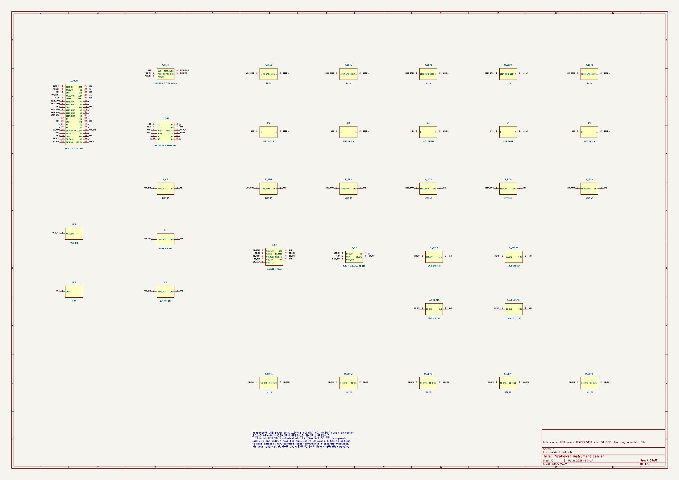
Open full-size schematic PNG · Download schematic PDF.
The EVM socket sits at the left edge, the Pico sockets in the middle, five LEDs along the right edge, and the hinged card socket in the lower-left. The JST-XH connector is above the EVM interface. Four mounting holes provide support on a shared bench base.
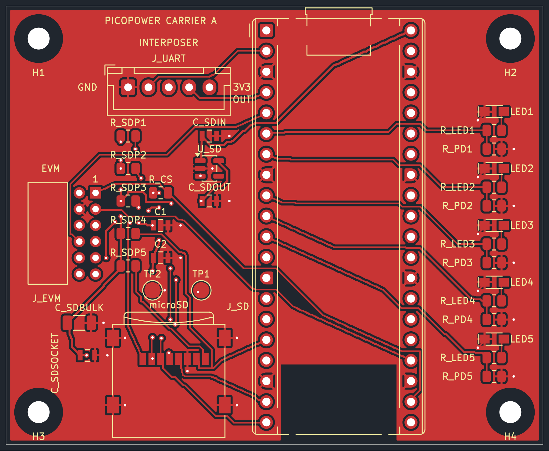
Open full-size PCB PNG · Original front SVG.
Open carrier.kicad_pro in KiCad 9. The schematic uses named nets: matching names are electrical connections. LED polarity is explicitly labelled A/K. J_PICO uses a combined socketed-Pico footprint; fit two 1x20 female strips at 17.78 mm row separation, with a compatible headered Pico. Its module/header height requires physical review.
make carrier-build deliberately overwrites carrier CAD and routes it again. Save interactive edits before using it. make carrier-check, make carrier-erc and make carrier-drc check the source/PCB mapping and native CAD. make carrier-export requires all checks to pass before exporting the review archive. Existing interposer build targets remain independent. These commands need KiCad 9, the distribution Python pcbnew module and NumPy.
LED1-LED5 use GP4-GP8 (physical pins 6, 7, 9, 10, 11), each with a 1 kOhm series resistor and a 100 kOhm GPIO pull-down. High turns an LED on; low turns it off. Firmware functions and PWM remain programmable. The LED datasheet gives typical Vf 2.65 V at 2 mA; using this voltage gives a 0.65 mA reference estimate per LED, not a solved operating point. Actual current and brightness remain bench checks. See the current calculations.
J_UART is JST B5B-XH-A(LF)(SN), with pins 1-5: GND, PICO_RX, PICO_TX, PICO_MARK, PICO_3V3. A straight-through five-wire harness uses XHP-5 housings at both ends and ten SXH-001T-P0.6 contacts. Pin 5 supplies the interposer buffer from the Pico. See the wiring procedure.
J_EVM is Sullins NPPN062FJFN-RC. Local pad numbering follows the TI-SCB mating interface: pin 4 GND, pin 6 3.3 V; pin 2 (5 V) is unconnected. Sullins drawing 10461-H gives 2 mm pitch, 0.8 mm drilling, 12.5 mm body width, 4.85 mm projected depth and 7.2 mm height. The saved outline now uses the corrected 4.85 mm depth; see the integrated footprint corrections. The drawing does not specify pin numbering; validate orientation and correspondence with EVM J3 before fabrication. Body offset, mating height and actual EVM revision remain subject to physical review. Pin 1 supplies CS; set the EVM's switch to that input. The EVM already includes the ALERT pull-up. Keep R1 empty and connect analog sensing directly from the interposer.
J_SD uses a hinged Würth 693072010801 socket on SPI1 (GP12-GP15), separate from INA229 SPI0. Five 10 kOhm pull-ups bias CMD/DAT0-DAT3. A TLV75533PDBVR supplies SD_3V3 from Pico USB VBUS, enabled by PICO_3V3, with 4.7 uF input/output capacitors and 22 uF/100 nF near the slot. The rails are not joined. The socket has no card-detect switch; recording requires future buffered logger firmware. See the storage and power details.
The board is 66 x 54 mm, 1.6 mm FR4, with two 35 um copper layers. Four 2.7 mm NPTH mounting holes at (4,4), (62,4), (4,50), (62,50) mm have 6 mm copper keepouts. Use M2.5 nylon hardware and independent supports for the EVM on a shared bench base; measure EVM support locations and match board height without stressing the connector. The antenna has a copper keepout on both sides; keep base material, metal hardware and cables clear of the antenna region. The EVM support pattern is intentionally not inferred from the reference photograph.
Engineering draft, not fabrication-ready. Automated reports describe CAD checks only. There are no released Gerbers, procurement actions or carrier firmware. Native footprints are snapshotted locally; the Sullins socket is a custom dimensional draft. Complete component/circuit/footprint/orientation review and physical mock-up before prototype fabrication; complete assembled-board electrical tests before DUT connection. The CSV checklist, release procedure and current review findings record both gates, which remain blocked.
KiCad 9.0.9 reports zero ERC violations, zero DRC violations, zero unconnected pads and zero schematic parity issues. Ten carrier regression tests cover connector mappings, LED GPIOs, separate SD power and SPI1 allocation; run them with the thirteen existing interposer tests. Re-run checks after edits; do not suppress violations to obtain a release.
With instrument and DUT supplies disabled, verify connector continuity, LED polarity and separation from DUT power. After electrical review, validate independent USB power and EVM 3.3 V before attaching DUT sense wiring. Exercise all five LEDs individually, together and with PWM; check reset behavior. Validate SPI device identification, ALERT, UART and marker signals, then card write/read checks and supply stability with SD writes, Wi-Fi and all indicators active. Measure card current peaks and regulator temperature; the 500 mA regulator rating is not a board-level continuous-load guarantee. Follow the existing interposer power-off procedure. Firmware/test tooling for these bench exercises is a separate milestone.
Record actual module/EVM revisions, socket height, supply voltages, traces, equipment and results. A Linux shutdown alone is not proof that Pi 3.3 V is off. Physical acceptance remains not performed.
| Qty | Value | Footprint | References |
|---|---|---|---|
| 6 | 100k 1% | Carrier:R_0805 | R_CS, R_PD1, R_PD2, R_PD3, R_PD4, R_PD5 |
| 5 | 10k 1% | Carrier:R_0805 | R_SDP1, R_SDP2, R_SDP3, R_SDP4, R_SDP5 |
| 5 | 1k 1% | Carrier:R_0805 | R_LED1, R_LED2, R_LED3, R_LED4, R_LED5 |
| 4 | MountingHole_2.7mm_M2.5 | Carrier:MountingHole_2.7mm_M2.5 | H1, H2, H3, H4 |
| 2 | 100nF X7R 16V | Carrier:C_0805_Murata | C_SDSOCKET, C1 |
| 2 | 4.7uF X7R 16V | Carrier:C_0805_Murata | C_SDIN, C_SDOUT |
| 1 | 1uF X7R 16V | Carrier:C_0805_Murata | C2 |
| 1 | 22uF X5R 16V | Carrier:C_1206 | C_SDBULK |
| 1 | 3.3V / dedicated SD LDO | Carrier:SOT23_5 | U_SD |
| 1 | GND | Carrier:TestPoint | TP2 |
| 1 | INA229EVM / direct plug | Carrier:NPPN062FJFN | J_EVM |
| 1 | INTERPOSER / JST-XH-5 | Carrier:XH5 | J_UART |
| 1 | LED1 GREEN | Carrier:LED_0805 | D1 |
| 1 | LED2 GREEN | Carrier:LED_0805 | D2 |
| 1 | LED3 GREEN | Carrier:LED_0805 | D3 |
| 1 | LED4 GREEN | Carrier:LED_0805 | D4 |
| 1 | LED5 GREEN | Carrier:LED_0805 | D5 |
| 1 | PICO 3V3 | Carrier:TestPoint | TP1 |
| 1 | Pico 2 W / socketed | Carrier:Pico_Socketed | J_PICO |
| 1 | microSD / hinge | Carrier:microSD_Wuerth | J_SD |
nherbaut/pico-power-sensor
This board sockets a Pico 2 W, provides five programmable green LEDs and a microSD slot, and connects to the INA229EVM through a left-edge right-angle socket.

Board-Folk/Neptune
Recreation of the cancelled Sega console that combines Mega Drive/Genesis with 32X.

bernardopg/ps28-modern-amp
Infinity Primus PS28 amplifier modernization: TPA3255 engineering, validation and safety-gated workflow

NOAA-PMEL/ASVCO2
Open Source Repository for the Autonomous Surface Vehicle CO2 (ASVCO2) gen2 system

sndsgd/er-tft0784-2-breakout
Test PCB for an ER-TFT0784-2 MIPI DSI display

Game-Team-SLSC/eurobot-2026-robot
The repo for firmware and hardware and docs of the 2026 Game Team's robot for CDFR Junior


kavanoz64/BeamBender-BigBox
An AGA digital scandoubler and HDMI output card for the Amiga 4000, with Amiga 2000 / 3000 support.

It measures 66 × 54 mm and has 2 copper layers, 1.6 mm thick.
38 parts, built around the CRCW0805100KFKEAC, CRCW080510K0FKEAC, CRCW08051K00FKEAC and CL31A226KOHNNNE. The full list of its parts is on this page, with links to each part's symbol and footprint where PCBKit's library has them.
From the nherbaut/pico-power-sensor repository on GitHub, at the commit this page was made from: the board is hardware/pcb/carrier/carrier.kicad_pcb and its schematic hardware/pcb/carrier/carrier.kicad_sch. PCBKit opens the board in the browser, with nothing to install.
Its repository states no licence, so its author keeps all rights: ask nherbaut before reusing the design.