4 layers100 × 80 mm
Open Beam Interface
nanographs/Open-Beam-Interface
Just what you need to control the beam and get an image.
334 parts371

 nanographs/Open-Beam-Interface371
Just what you need to control the beam and get an image.
Open Beam Interface is an open-source printed circuit board by nanographs, from the nanographs/Open-Beam-Interface repository on GitHub. It is a 4-layer board of 100 × 80 mm with 334 parts on 235 nets, routed with 2,117 tracks and 452 vias.
It is built around the AD9744ARUZ, THS4151ID and AD8137YRZ, with the LTC2246HLX#PBF, 74ALVCH16373DGG:11 and LT3045EDD among its other parts. Its parts include 100 resistors, 88 capacitors, 20 ICs, 14 diodes and 8 connectors. It belongs with the interfaces and adapters boards of this library.


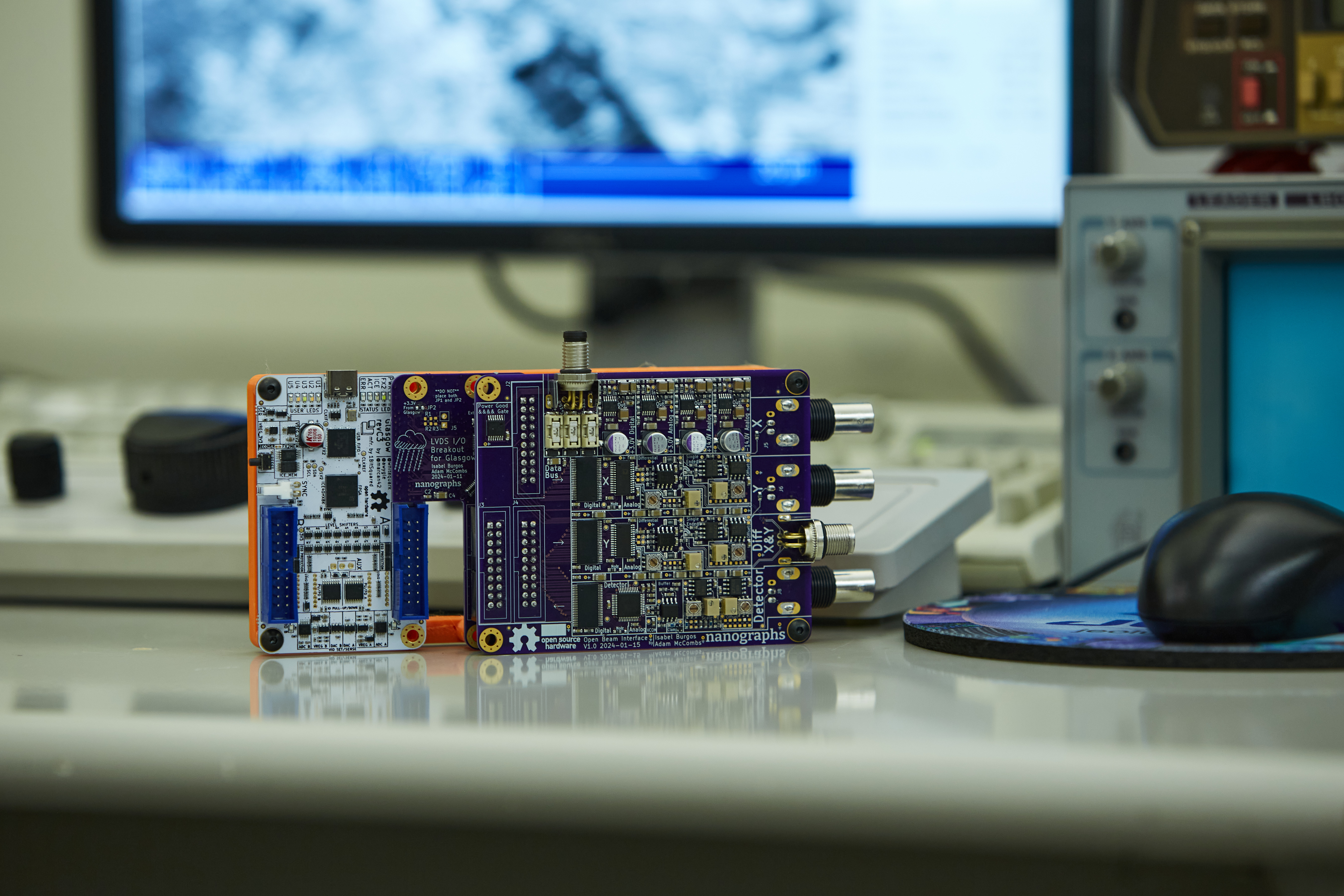
Check out our docs at https://nanographs.github.io/Open-Beam-Interface/index.html
The Open Beam Interface project aims to make getting data into and out of scanning and patterning systems substantially more accessible. It is applicable to a variety of scanning and patterning systems but is especially useful for electron and ion microscopes.
Two high-speed digital-to-analog converters position the beam in X and Y and a high-speed analog-to-digital converter acquires the signal from a detector.
Just what you need to control the beam and get an image.
Built on Glasgow, written in Amaranth.
Glasgow makes getting bytes in and out of the FPGA over USB radically more accessible. We use that to make getting data into and out of your microscope radically more accessible.
Glasgow handles getting the bytes in and out of your computer. Our software takes those bytes and forms an image, while simultaneously streaming bytes to Glasgow to support raster and vector patterning applications.

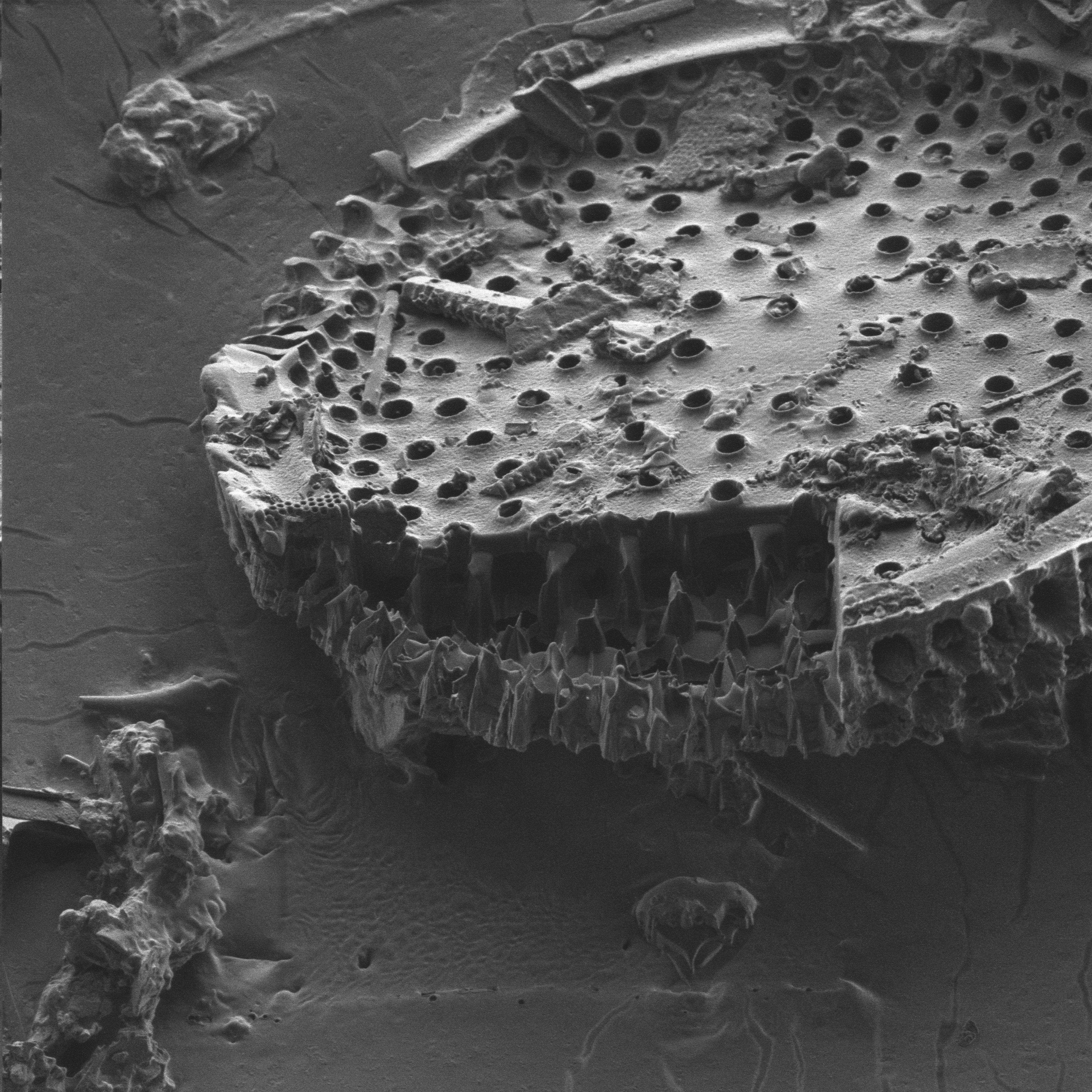
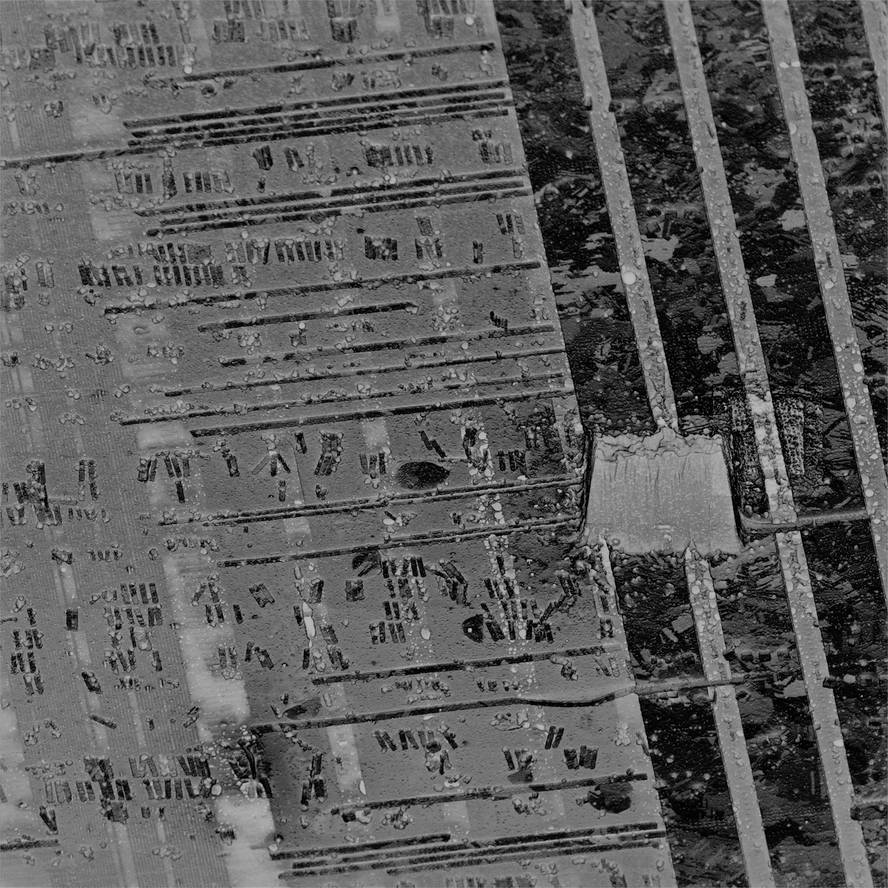
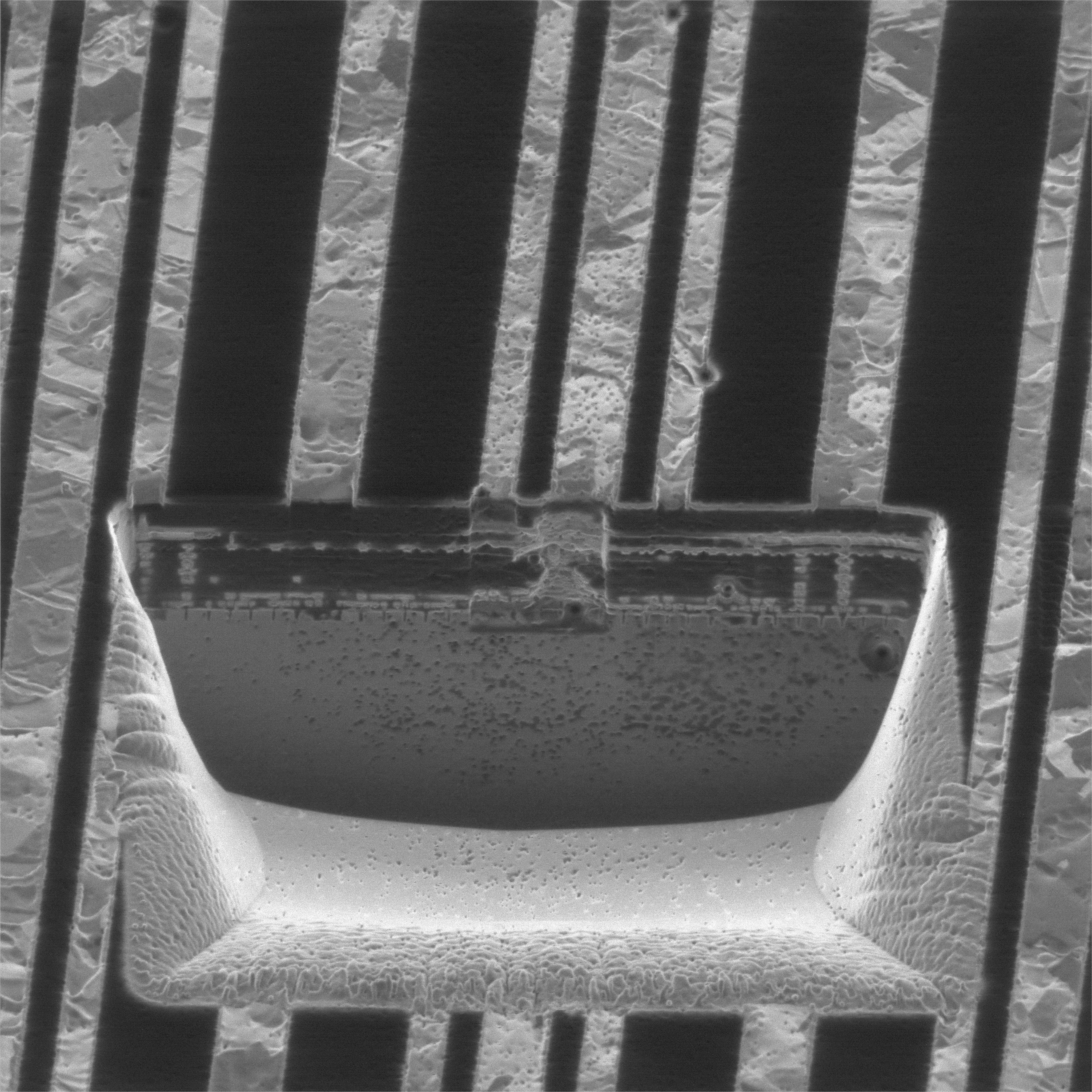
We have crafted this board to support as many microscopes as possible. We do not know of a SEM or FIB that specifically does not have these signals somewhere inside that can be tapped.
Many microscopes have an existing dedicated connector for external scan inputs. Originally, this was generally for external beam control coming from EDS or other X-Ray mapping systems.
For microscopes that do not have a dedicated external scan connector, the X and Y ramps that drive the scan coils exist somewhere. A relay can be installed to flip between internal and external scan. Sometimes, even when microscopes have a dedicated connector, it is better to tap the X and Y signals somewhere else.
Has a XY scan input that is either:
Has a video output that is:
Tapping into the signal path may require fabricating a custom cable.
Microscopes the board has been specifically integrated into, this is far from an exhaustive list of microscopes that we could interface with.
We would like to thank our sponsors' generous sustaining contributions. Without them, we would not be here today.
We are always open to potential microscope donations to use for hardware development, in order to expand the range of microscopes and capabilities we can support. Right now we are especially in search of FIBs, Dual Beams, and TEMs.
Thanks to the generous support of our financial sponsors, we have been able to dedicate almost all of our time and facility resources to developing the project this far. We are looking for more sponsors in order to continue our work, involve more engineers, and take this project to the next level.
Superior Technical Services
SEMion
CERN-OHL-W
| Qty | Value | Footprint | References |
|---|---|---|---|
| 44 | 0.1 uF | Capacitor_SMD:C_0603_1608Metric | C12, C13, C15, C16, C24, C26, C27, C28, C29, C31, C32, C34, C35, C36, C37, C38 +28 |
| 34 | TestPoint | TestPoint:TestPoint_Pad_D1.0mm | PowerGood1, TP_A-1, TP_A+1, TP_A3.1, TP_ADC_MSB1, TP_Clamped1, TP_Clk_A1, TP_Clk_D2, TP_D3.1, TP_IA_X1, TP-1, TP-2, TP+1, TP+2, TP+3.1, TP+3.2 +18 |
| 26 | TestPoint | Scan Generator:GND Test Point WIth Dimensions | GNDA1, GNDA2, GNDA3, GNDA4, GNDA5, GNDA6, GNDA7, GNDA8, GNDA10, GNDA11, GNDA12, GNDA13, GNDA14, GNDA15, GNDA16, GNDA17 +10 |
| 23 | 4.7u | Capacitor_SMD:C_1206_3216Metric | C3, C4, C5, C6, C14, C17, C21, C22, C33, C42, C43, C62, C63, C64, C73, C75 +7 |
| 13 | R | Resistor_SMD:R_0603_1608Metric | R65, R68, R69, R71, R72, R74, R76, R77, R78, R79, R80, R82, R96 |
| 12 | 1K | Resistor_SMD:R_0603_1608Metric | R5, R17, R43, R44, R49, R52, R53, R54, R55, R56, R57, R94 |
| 11 | 10k | Resistor_SMD:R_0603_1608Metric | R6, R8, R11, R13, R18, R20, R22, R85, R88, R99, R100 |
| 8 | LED | LED_SMD:LED_0603_1608Metric | D1, D2, D3, D4, D5, D6, D8, D9 |
| 6 | 0 | Resistor_SMD:R_0603_1608Metric | R47, R48, R50, R51, R62, R63 |
| 6 | 10K | Resistor_SMD:R_0603_1608Metric | R23, R24, R25, R26, R97, R98 |
| 6 | 25 | Resistor_SMD:R_0603_1608Metric | R31, R32, R33, R34, R35, R36 |
| 6 | LT1363 | Scan Generator:SOIC-8_3.9x4.9mm_P1.27mm | U13, U14, U15, U16, U17, U18 |
| 6 | ~ | Scan Generator:Nidec SP4T CS-4-14NTA | SW1, SW2, SW3, SW4, SW5, SW6 |
| 5 | 20K | Potentiometer_SMD:Potentiometer_Bourns_3224W_Vertical | RV1, RV2, RV5, RV6, RV7 |
| 4 | 1.82K | Resistor_SMD:R_0603_1608Metric | R59, R60, R75, R81 |
| 4 | 100 uF | Scan Generator:CAP_20SVPF120M | C7, C8, C9, C10 |
| 4 | 10u | Capacitor_SMD:C_1210_3225Metric | C1, C2, C11, C46 |
| 4 | 10u | Scan Generator:C_1210_3225_Kelvin_Connections | C18, C19, C20, C25 |
| 4 | 13K | Resistor_SMD:R_0603_1608Metric | R7, R9, R15, R21 |
| 4 | 301 | Resistor_SMD:R_0603_1608Metric | R37, R38, R39, R40 |
| 4 | 4.99K | Resistor_SMD:R_1206_3216Metric | R41, R42, R45, R46 |
| 4 | FerriteBead | Inductor_SMD:L_0603_1608Metric | FB1, FB2, FB3, FB4 |
| 4 | MMBT3904TT1G | Scan Generator:SOT-416 | Q1, Q2, Q3, Q4 |
| 4 | MountingHole | Scan Generator:MountingHole_3.5mm_Pad_Via_CrtYd | H1, H2, H3, H4 |
| 3 | 2.2 uF | Capacitor_SMD:C_0603_1608Metric | C30, C52, C54 |
| 3 | 500 | Resistor_SMD:R_0603_1608Metric | R58, R61, R64 |
| 3 | 74ALVCH16373DGG:11 | Package_SO:TSSOP-48_6.1x12.5mm_P0.5mm | U4, U5, U6 |
| 3 | Coaxial Con Amphenol 031-5538-10RFX | Scan Generator:BNC_Amphenol_B6252HB-NPP3G-50_Horizontal_Flipable | J5, J6, J8 |
| 3 | Conn_02x10_Odd_Even | Scan Generator:IDC-Header_2x10_P2.54mm_Vertical_No_Pin_1_Mark | J2, J3, J4 |
| 3 | Fiducial | Fiducial:Fiducial_0.75mm_Mask1.5mm | FID1, FID2, FID3 |
| 3 | Fuse_Holder | Scan Generator:01550900M | FH1, FH2, FH3 |
| 3 | Jumper_3_Bridged12 | Scan Generator:R_0603_1608Metric 2 pos sellector | JP5, JP6, JP7 |
| 3 | LT3045 | Package_SO:MSOP-12-1EP_3x4mm_P0.65mm_EP1.65x2.85mm_ThermalVias | U1, U2, U19 |
| 3 | SMF20A | Diode_SMD:D_SMF | D10, D11, D12 |
| 2 | 1 uF | Capacitor_SMD:C_0603_1608Metric | C58, C59 |
| 2 | 1.5K | Resistor_SMD:R_0603_1608Metric | R4, R84 |
| 2 | 140k | Resistor_SMD:R_0603_1608Metric | R2, R16 |
| 2 | 2.49K | Resistor_SMD:R_0603_1608Metric | R29, R30 |
| 2 | 3.3K | Resistor_SMD:R_0603_1608Metric | R3, R89 |
| 2 | 33k | Resistor_SMD:R_0603_1608Metric | R1, R83 |
| 2 | 392K | Resistor_SMD:R_0603_1608Metric | R12, R19 |
| 2 | 5K | Resistor_SMD:R_0603_1608Metric | R66, R67 |
| 2 | 68.1 | Resistor_SMD:R_0603_1608Metric | R14, R86 |
| 2 | 90.9K | Resistor_SMD:R_0603_1608Metric | R10, R87 |
| 2 | AD9744ARUZ | Package_SO:TSSOP-28_4.4x9.7mm_P0.65mm | U7, U8 |
| 2 | C-Opt | Capacitor_SMD:C_0603_1608Metric | C51, C55 |
| 2 | OSHW-Logo_11.4x12mm_SilkScreen | Symbol:OSHW-Logo_11.4x12mm_SilkScreen | OSHW_logo_back, OSHW_logo_front |
| 2 | R | Scan Generator:Reduced_pads_R_Axial_DIN0204_L3.6mm_D1.6mm_P5.08mm_Horizontal | R70, R73 |
| 2 | THS4151 | Scan Generator:HVSSOP-8-1_Expanded_Thermal_Pad_P0.65mm_EP1.57x1.89mm_ThermalVias | U11, U12 |
| 1 | 10.2k | Resistor_SMD:R_0603_1608Metric | R27 |
| 1 | 10.5k | Resistor_SMD:R_0603_1608Metric | R92 |
| 1 | 12 pF | Capacitor_SMD:C_0603_1608Metric | C50 |
| 1 | 12.1k | Resistor_SMD:R_0603_1608Metric | R91 |
| 1 | 14k | Resistor_SMD:R_0603_1608Metric | R90 |
| 1 | 18.7k | Resistor_SMD:R_0603_1608Metric | R93 |
| 1 | 2K | Potentiometer_SMD:Potentiometer_Bourns_3224W_Vertical | RV3 |
| 1 | 2K | Resistor_SMD:R_0603_1608Metric | R95 |
| 1 | 37.4k | Resistor_SMD:R_0603_1608Metric | R28 |
| 1 | 7430 | Package_SO:TSSOP-14_4.4x5mm_P0.65mm | U20 |
| 1 | AD8137YRZ | Scan Generator:SOIC-8_3.9x4.9mm_P1.27mm | U10 |
| 1 | C | Capacitor_SMD:C_0603_1608Metric | C74 |
| 1 | Cable Pinout 1-8 Back | Scan Generator:Cable Pinout 1-8 Back | D1-D8_silk_labels |
| 1 | Cable Pinout 9-16 Back | Scan Generator:Cable Pinout 9-16 Back | D9-D16_silk_labels |
| 1 | Cable Pinout Ctrl Back | Scan Generator:Cable Pinout Ctrl Back | ctrl_silk_labels |
| 1 | Conn_01x04_Shielded | Scan Generator:Female M8 Right Angle Panel Mount Connector | J7 |
| 1 | Conn_01x04_Shielded | Scan Generator:M8 Right Angle Panel Mount Connector | J1 |
| 1 | LOGO | Scan Generator:Portland Oregon Stag Sign | PDX_sign |
| 1 | LT3094_MSE | Package_SO:MSOP-12-1EP_3x4mm_P0.65mm_EP1.65x2.85mm_ThermalVias | U3 |
| 1 | LTC2246HLX#PBF | Package_QFP:LQFP-48_7x7mm_P0.5mm | U9 |
| 1 | Nanographs Big | Scan Generator:Nanographs Big | back_logo |
| 1 | Offset and Scale Drawing | Scan Generator:Offset and Scale Drawing | offset_scale_single_diff_drawing |
| 1 | SS423(TE85L,F) | Scan Generator:SOT-416 | D7 |
| 1 | Scan Gen Art 2 | Scan Generator:Scan Gen Art 2 | scanning_art |
| 1 | nanographs small | Scan Generator:nanographs small | front_logo |
The 331 most common of 334 parts.
It measures 100 × 80 mm and has 4 copper layers, 1.57 mm thick.
334 parts, built around the AD9744ARUZ, THS4151ID, AD8137YRZ and LTC2246HLX#PBF. The full list of its parts is on this page, with links to each part's symbol and footprint where PCBKit's library has them.
From the nanographs/Open-Beam-Interface repository on GitHub, at the commit this page was made from: the board is Hardware/PCBs/Open Beam Interface/Open Beam Interface revA3/Open Beam Interface.kicad_pcb and its schematic Hardware/PCBs/Data Interconnect/Data Interconnect revA1/OBI Data Interconnect.kicad_sch. PCBKit opens the board in the browser, with nothing to install.
Its repository states no licence, so its author keeps all rights: ask nanographs before reusing the design.
nanographs/Open-Beam-Interface
Just what you need to control the beam and get an image.

nanographs/Open-Beam-Interface
Just what you need to control the beam and get an image.

nanographs/Open-Beam-Interface
Just what you need to control the beam and get an image.

nanographs/Open-Beam-Interface
Just what you need to control the beam and get an image.

nanographs/Open-Beam-Interface
Just what you need to control the beam and get an image.

nanographs/Open-Beam-Interface
Just what you need to control the beam and get an image.

nanographs/Open-Beam-Interface
Just what you need to control the beam and get an image.

nanographs/Open-Beam-Interface
Just what you need to control the beam and get an image.

nanographs/Open-Beam-Interface
Just what you need to control the beam and get an image.

nanographs/Open-Beam-Interface
Just what you need to control the beam and get an image.


Joe-Purvis/UFE
This repository consolidates multiple projects into a single monorepo for the Ultrasound Smart Switch system.

LongDo1902/STM32_Drone
Developing quadcopter from scratch including stm32 programing and self-built flight controller PCB.

ymhtwe/SGW01
ESP-IDF based IoT gateway for solar pump monitoring and control using SIM7600 4G modem and Modbus RTU.

OpenLogicEFI/Hardware
Hardware is based off an open source project called Speeduino by Josh Stewart.

blonski3/ibm-modern-m-ssk
Decyzje projektowe i ich uzasadnienia: docs/HARDWAREDECISIONS.md; historia zmian: docs/CHANGELOG.md.

Fluffik214/airsoft-battery-module
This is a USB-C PD charger and cell monitor for a 3S LiPo that lives in an airsoft stock tube. It has one USB-C port.

fulgidus/hardware
Learning KiCad takes time, and pollutes with weird and incomplete projects. Here they are...