2 layers310.8 × 106.1 mm

 nanbuwks/QuinoaChipPlant
キヌア( Quinua ):南米で食されている雑穀。 栄養的に優れていて、スーパーフードとして注目されている。 乾燥/湿地、低温、塩地などの他の作物が育たない環境でも栽培ができる。 遺伝子が多様で、品種改良が期待される。
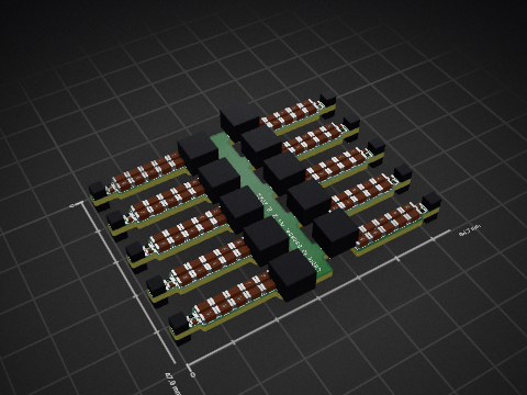
QuinoaChipPlant is an open-source printed circuit board by nanbuwks, from the nanbuwks/QuinoaChipPlant repository on GitHub. It is a 2-layer board of 180 × 263.2 mm with 150 parts on 71 nets, routed with 1,228 tracks and 61 vias.
Its parts include 20 diodes, 19 resistors, 18 connectors, 17 capacitors and 9 ICs. It belongs with the ESP32 boards of this library.
キヌアの育種のために、撒種→結実を速いサイクルで回すためのプラントです。
キヌア( Quinua ):南米で食されている雑穀。 栄養的に優れていて、スーパーフードとして注目されている。 乾燥/湿地、低温、塩地などの他の作物が育たない環境でも栽培ができる。 遺伝子が多様で、品種改良が期待される。
1つのチップに1粒ずつ撒種し、水耕栽培を行います。 1つのラックにチップが24収納できますが、チップ1つ分はセンサーのために使うので1つのラックで23粒を撒きます。 芽が出たら1つのラックに10程度に間引きします。 100ラックで実験するとなると、1000株を育成することになります。 収量を目的とするのではなく、促成で種を回収することを目的としています。
水換え、光照射、センサ接続ができるロボットボードです。 1000株分を育成するのは水替えも大変なので、自動で水換えを行います。 プログラムで自動運転できるので、一時冠水を繰り返すような運転を行うことができます。
「キヌア栽培のための制御回路をつくってみよう」 https://qiita.com/nanbuwks/items/138a8bbda59f0657b9df
discord OpenHardTerrace 中の #chipplant で開発しています。 https://discord.gg/T8mKzFyu6m
| Qty | Value | Footprint | References |
|---|---|---|---|
| 47 | MountingHole_3.2mm_M3 | MountingHole:MountingHole_3.2mm_M3 | REF08, REF08, REF10, REF11, REF12, REF12, REF12, REF100, REF111, REF112, REF113, REF114, REF115, REF116, REF117, REF119 +31 |
| 14 | 470 | Resistor_SMD:R_1206_3216Metric_Pad1.30x1.75mm_HandSolder | R3, R4, R5, R6, R11, R12, R13, R14, R15, R16, R17, R18, R19, R20 |
| 11 | C | Resistor_SMD:R_1206_3216Metric_Pad1.30x1.75mm_HandSolder | C6, C7, C8, C9, C10, C11, C12, C13, C14, C16, C17 |
| 10 | D | Diode_SMD:D_SOD-123 | D1, D2, D3, D4, D5, D6, D7, D10, D11, D18 |
| 10 | LED | LED_THT:LED_D3.0mm | D8, D9, D12, D13, D14, D15, D16, D17, D19, D20 |
| 8 | , , , , , , , | ||
| 6 | BULB | Connector_JST:JST_XH_B2B-XH-AM_1x02_P2.50mm_Vertical | J7, J8, J9, J10, J15, J16 |
| 5 | SparkFun_TB6612FNG_MOTOR_DRIVER_MODULE | library:SparkFun_TB6612FNG_MOTOR_DRIVER_MODULE | U2, U3, U4, U6, U8 |
| 4 | 10K | Resistor_SMD:R_1206_3216Metric_Pad1.30x1.75mm_HandSolder | R7, R8, R9, R10 |
| 3 | C_Polarized | Capacitor_THT:CP_Radial_D10.0mm_P2.50mm_P5.00mm | C2, C4, C15 |
| 2 | C | Capacitor_SMD:C_1206_3216Metric_Pad1.33x1.80mm_HandSolder | C1, C3 |
| 2 | GROVE | Connector_JST:JST_PH_B4B-PH-K_1x04_P2.00mm_Vertical | J1, J18 |
| 2 | MOTOR | Connector_JST:JST_XH_B2B-XH-AM_1x02_P2.50mm_Vertical | J5, J6 |
| 2 | MountingHole_4.3mm_M4_DIN965 | MountingHole:MountingHole_4.3mm_M4_DIN965 | REF07, REF09 |
| 2 | Screw_Terminal_01x04 | TerminalBlock_Phoenix:TerminalBlock_Phoenix_PT-1,5-4-5.0-H_1x04_P5.00mm_Horizontal | J4, J20 |
| 1 | 0.1uF | Capacitor_SMD:C_1206_3216Metric_Pad1.33x1.80mm_HandSolder | C5 |
| 1 | Buzzer | Buzzer_Beeper:Buzzer_12x9.5RM7.6 | BZ1 |
| 1 | CR2013-MI2120 | library:TFT3.2_ILI9341 | U7 |
| 1 | DCJACK | library:DCJACK | J2 |
| 1 | DCJACK OPTIONAL | library:DCJACK | J14 |
| 1 | ESP32_DEVKIT_V1 | library:ESP32_DEVKIT_V1 | U1 |
| 1 | LEVEL1 | Connector_JST:JST_XH_B4B-XH-AM_1x04_P2.50mm_Vertical | J3 |
| 1 | LEVEL2 | Connector_JST:JST_XH_B4B-XH-AM_1x04_P2.50mm_Vertical | J11 |
| 1 | LEVEL3 | Connector_JST:JST_XH_B4B-XH-AM_1x04_P2.50mm_Vertical | J12 |
| 1 | LEVEL4 | Connector_JST:JST_XH_B4B-XH-AM_1x04_P2.50mm_Vertical | J13 |
| 1 | MountingHole_8.4mm_M8 | MountingHole:MountingHole_8.4mm_M8 | USB Cable |
| 1 | OSHW-Logo2_9.8x8mm_SilkScreen | Symbol:OSHW-Logo2_9.8x8mm_SilkScreen | REF118 |
| 1 | R | Resistor_SMD:R_1206_3216Metric_Pad1.30x1.75mm_HandSolder | R1 |
| 1 | SEEED_GROVE | library:Seeedstudio_Grove_110990030_Vertical_4pin_2mmpitch | U5 |
| 1 | SW_Push | Button_Switch_THT:SW_PUSH_6mm | SW1 |
| 1 | SolderJumper_2_Bridged | Jumper:SolderJumper-2_P1.3mm_Bridged_Pad1.0x1.5mm | JP3 |
| 1 | Thermistor | TerminalBlock_Phoenix:TerminalBlock_Phoenix_MKDS-1,5-2_1x02_P5.00mm_Horizontal | TH1 |
| 1 | ~ | library:YRB_YMD-10WR3_YRA_YMD-10WR3 | U9 |
The 146 most common of 150 parts.

Nakazoto/CenturionComputer
This is just a simple backup of all the files related to the Centurion that I have stored on my HD. The Wiki itself has far more in-depth information about the Centurion and it's individual cards.

johanwheeler/ch32-fireplace
Ch32 based christmas card with 8x8 screen, sound and capacitive buttons

shabaz123/pico-eurocard
This repository contains PCB Gerber files and bill of materials for a Pi Pico Eurocard Development Board. See James' Workshop Wednesday's Video which demonstrates the revision 2.0 board.

eightbitraptor/65_keyboard_untitled
My as yet unnamed 65% keyboard design

lynchaj/duodyne
Duodyne is a hobbyist retrocomputer system designed to run ROMWBW. It is comprised of modules on a system bus

It measures 180 × 263.2 mm and has 2 copper layers, 1.6 mm thick.
150 parts. The full list of its parts is on this page, with links to each part's symbol and footprint where PCBKit's library has them.
From the nanbuwks/QuinoaChipPlant repository on GitHub, at the commit this page was made from: the board is KiCad/QuinoaChipPlant.kicad_pcb and its schematic KiCad/QuinoaChipPlant.kicad_sch. PCBKit opens the board in the browser, with nothing to install.
Its repository states no licence, so its author keeps all rights: ask nanbuwks before reusing the design.