4 layers145.4 × 99.1 mm
Esp32 xiaozhi
siliconvalleyar-oss/esp32_xiazhi_pcb
Repositorio del diseño PCB para el dispositivo XiaoZhi, una estación de desarrollo y asistente de voz de código abierto basado en el ESP32-C6.
235 parts

 n2048-creative-technology/esp32-led-matrix
double sided 8x8 addressable led matrix with integrated esp32-c3 module
Esp32-led matrix is an open-source printed circuit board by n2048-creative-technology, from the n2048-creative-technology/esp32-led-matrix repository on GitHub. It is a 2-layer board of 58.1 × 41.8 mm with 147 parts on 163 nets, routed with 1,472 tracks and 38 vias.
It is built around the ESP32-C6-WROOM-1-N8, LM1117DT-3.3 and USBLC6-2SC6, with the WS2812B among its other parts. Its parts include 130 diodes, 6 capacitors, 5 resistors, 3 ICs and 2 connectors. It belongs with the lEDs and displays boards and the ESP32 and RISC-V boards of this library.


Double-sided 8x8 WS2812B LED matrix board driven by an ESP32-C6-WROOM-1, powered over USB-C. This design merges the MCU/power subsystem from esp32-ce-led with the LED-matrix/JST-PH-connector pattern from xiao-led-module-, extended to a double-sided 8x8 array (128 total LEDs, two independent 64-LED daisy chains on GPIO6/GPIO7 — one per board side).
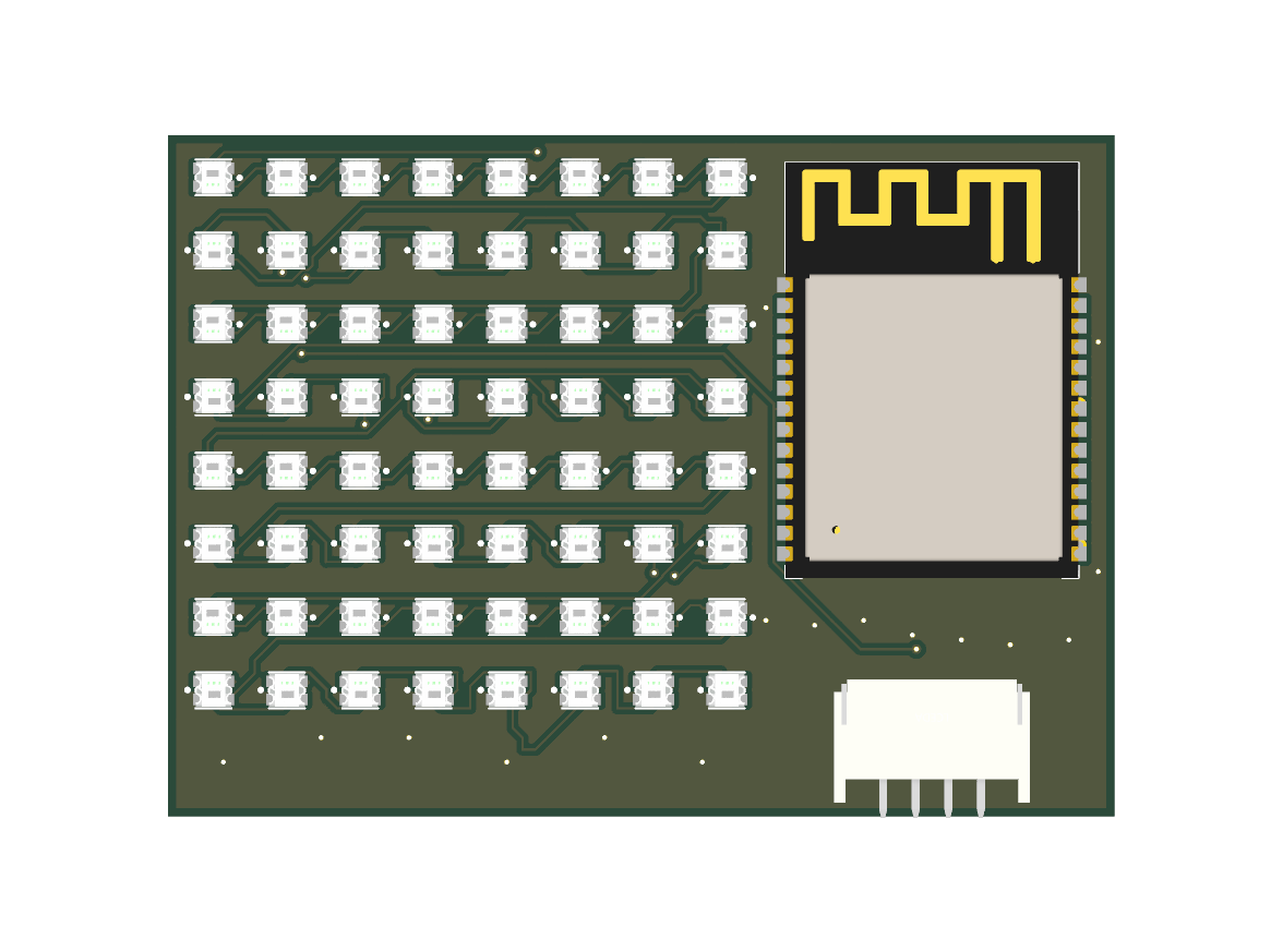
| MCU | ESP32-C6-WROOM-1-N8 (Wi-Fi 6 / BLE 5, RISC-V) |
| Power in | USB-C (5V), on-board AMS1117-3.3 regulator for MCU rail |
| LED driver rail | +5V direct from USB-C (WS2812B needs ~5V, not 3.3V) |
| LEDs | 128x WS2812B-2020, 8x8 grid on F.Cu + 8x8 grid on B.Cu |
| LED chains | Chain A: D10→D73 (64 LEDs, GPIO6) · Chain B: D74→D137 (64 LEDs, GPIO7) |
| USB protection | USBLC6-2SC6 ESD array on D+/D-, ESD9B3.3ST5G on VBUS |
| Status | Power LED (D1), reset button (SW1) |
| External power option | JST-PH 4-pin connector (J2) for +5V/GND injection |
| Layers | 2 (F.Cu / B.Cu), GND + 5V copper pours on both sides |
| Board size | 58.1 x 41.84mm (compact redesign — was 46 x 91mm; see LAYOUT_SPEC.md §1 for the height derivation — the B.Cu component stack, not the LED grid, drives the 41.84mm figure) |
| Layout | ESP32-C6 alone on F.Cu beside LED matrix A; USB-C/JST/regulator/ESD/switch/passives on B.Cu beside LED matrix B. USB-C (J4) centered on the right edge; JST (J2) at the bottom edge. See LAYOUT_SPEC.md for exact coordinates. |
Component numbering is intentional: D1 and D4 are reused from the MCU/power subsystem (status LED, ESD diode); D10 through D137 are the 128 matrix LEDs. The gap (D2/D3, D5–D9) is not a bug.
Full JLCPCB-verified BOM with LCSC part numbers: BOM_jlcpcb_verified.csv
(also duplicated as production/bom.csv in JLCPCB
upload format: Reference/Value/Footprint/LCSC/MPN/Manufacturer).
| Ref | Part | Qty | LCSC |
|---|---|---|---|
| U1 | ESP32-C6-WROOM-1-N8 | 1 | C5366877 |
| U2 | USBLC6-2SC6-FS | 1 | C6807798 |
| U3 | AMS1117-3.3 (TO-252) | 1 | C41347676 |
| D1 | Status LED (red, 0603) | 1 | C2286 |
| D4 | ESD9B3.3ST5G | 1 | C96512 |
| D10-D137 | WS2812B-2020 (compatible) | 128 | C5349955 |
| SW1 | Tactile switch (B3U-1000P) | 1 | C231329 |
| J4 | USB-C receptacle 16-pin | 1 | C3020560 |
| J2 | JST-PH 4-pin connector | 1 | C3029442 |
| R1, R2 | 5.1K 0402 | 2 | C25905 |
| R3 | 1K 0402 | 1 | C11702 |
| R7, R8 | 10K 0402 | 2 | C25744 |
| C1, C6 | 100nF 01005 | 2 | C307376 |
| C2, C3 | 22uF 0805 | 2 | C129302 |
| C4 | 1uF 0603 | 1 | C15849 |
| C5 | 10uF 0603 | 1 | C7472959 |
Every part is Basic/Extended JLCPCB stock with a verified LCSC number; no DNP parts in this design.
Every symbol/footprint used is confirmed installed via KiCad's Plugin and
Content Manager on this machine (checked against the global
sym-lib-table/fp-lib-table):
PCM_SparkFun-LED / PCM_SparkFun-Connector — SparkFun-KiCad-Libraries
(provides the WS2812B_2020 addressable LED and JST-PH 4-pin connector)PCM_Espressif — Espressif kicad-libraries (ESP32-C6-WROOM-1 module)Device, Connector, Power_Protection,
Regulator_Linear, Switch, Capacitor_SMD, Resistor_SMD, etc.) are
built into KiCad 9 by default.Opening this project on another machine requires installing the SparkFun and Espressif libraries via KiCad's Plugin and Content Manager first (Tools → Plugin and Content Manager → search "SparkFun" / "Espressif" → Install).
JLCPCB-verified alternate library (lib_jlcpcb/): both the
LED (XL-2020RGBC-2812B, LCSC
C5349955, 128,513
units in stock) and the JST-PH connector (WAFER-PH2.0-4PWB, LCSC
C3029442, 45,706
units in stock) were re-verified live against the JLCPCB Open Platform API
and a complete symbol+footprint+3D-model bundle was generated directly from
LCSC's EasyEDA source data via
easyeda2kicad — each part's
kicad_sym carries its live datasheet URL
(lcsc.com/datasheet/<LCSC#>.pdf) and LCSC part number as a property, and
jlcpcb_parts.3dshapes/ has real STEP/WRL 3D models for both parts.
WS2812_2020) already
has a complete, working datasheet link and real STEP 3D model on disk —
it was left as-is; swapping 128 LED placements to the new footprint
would touch copper on an already-fragile routed board for no functional
gain (pad geometry is compatible in function but not identical in size).JST_1x04_P2.0mm_Horizontal_SMD) was missing any 3D model — this was
fixed by attaching the new verified STEP model
(lib_jlcpcb/jlcpcb_parts.3dshapes/CONN-SMD_4P-P2.00_XUNPU_WAFER-PH2.0-4PWB.step)
directly to the existing footprint instance, a cosmetic-only change (no
pad/copper edits — DRC results unchanged, verified before/after: 100
violations / 61 unconnected in both cases). A full footprint swap was
considered but rejected: the new part's pad sizes and mounting-pad
layout differ from the current footprint, and a blind swap risked a real
mechanical mismatch rather than just a cosmetic one.Fabrication package in production/:
gerbers.zip — full Gerber set + drill file (gerbers/)bom.csv — JLCPCB-format BOMpositions.csv — CPL (component placement, both sides, mm)Board is 2-layer, JLCPCB-standard stackup, no exotic requirements.
DRC (kicad-cli pcb drc), after the compact-layout redesign (task series 1-7): board outline/LED-grid repositioning → ESP32 repositioning → B.Cu component repositioning → stale-copper clear → Freerouting re-route + GND/+5V zones → final cleanup:
| Stage | Violations | Unconnected items |
|---|---|---|
| Original layout, before redesign | 100 (100 lib_footprint_mismatch only) | 61 |
| After Freerouting re-route on new 58.1x41.84mm layout (task 6) | 382 (130 shorting_items, 130 solder_mask_bridge, 100 lib_footprint_mismatch, 9 items_not_allowed, 5 silk_overlap, 4 silk_over_copper, 2 copper_edge_clearance, 1 clearance, 1 via_dangling) | 312 |
| Final (task 7, this cleanup) | 128 (100 lib_footprint_mismatch, 9 items_not_allowed, 5 silk_overlap, 4 silk_over_copper, 3 shorting_items, 3 solder_mask_bridge, 2 copper_edge_clearance, 1 clearance, 1 via_dangling) | 189 |
Most of the task-6 regression (382→128 violations) turned out to be a
stale zone fill, not real routing damage: Freerouting's SES import left
the GND/+5V copper pours unfilled, so DRC flagged hundreds of phantom
clearance/short violations against zone outlines that had no actual copper
yet. A single zone refill (ZONE_FILLER.Fill()) cleared the bulk of it.
The remaining 28 non-lib_footprint_mismatch violations are genuine and
documented, not routing bugs introduced by this redesign:
LAYOUT_SPEC.md §10, physically overlap the ESP32's antenna-keepout zone
on B.Cu. This is a placement conflict from an earlier task in the series,
out of scope to fix here without moving U2/U3/re-deriving the layout spec.All 128 LED daisy-chain SIGNAL nets are fully routed except two short
inter-LED gaps that Freerouting's SES import missed: Net-(D79-DOUT) was
hand-routed clean in this task (0 new violations, verified via
per-segment clearance checks before committing); Net-(D81-DOUT) remains
open (D81↔D82 is a long cross-board run through very dense B.Cu daisy-chain
copper — safer to hand off for a proper autorouter pass than risk another
hand-routed short in this pitch). Of the 189 unconnected items, 178 are
zone-to-zone (GND/+5V copper-pour) stitching gaps — cosmetic DRC noise from
a segmented pour, not missing electrical connections, since both zones
already blanket most of each layer. The remaining ~11 are genuine point-to-
point gaps: Net-(D81-DOUT) (above), USB_D+/USB_D- to U2 (blocked by the
same antenna-keepout placement conflict as above — U2's D+/D- pads sit
inside the keepout, so no track can legally terminate there without moving
U2), U3's +3V3 pin (same keepout conflict), and D1's status-LED signal
net to R3 (D1 was moved off-board during this cleanup — it had been left
at y=53mm, outside the 41.84mm board height, a leftover coordinate bug from
the original schematic; now relocated to a clear F.Cu spot at (51, 36) but
not yet routed to R3 across the dense J2/passives cluster).
Recommended follow-up before fab: (1) resolve the U2/U3-vs-antenna-
keepout placement conflict — either shrink/move the keepout zone per the
antenna's real RF requirements or nudge U2/U3 clear of it; (2) run one more
Freerouting pass focused on Net-(D81-DOUT) and the D1→R3 net; (3) hand-
place a handful more GND stitching vias at the remaining zone-pour gaps (16
were added in this task at clear board locations — spread across the
bottom margin, right edge, and mid-board — reducing the stitching-gap count
but a fully-zero unconnected count would need more targeted work than this
pass's budget allowed).
ERC (kicad-cli sch erc): 78 violations, all benign/expected, IDENTICAL to
the pre-redesign baseline — the schematic was never touched by this PCB
layout redesign (only footprint positions changed), so ERC output matches
byte-for-byte: unused ESP32-C6 GPIO pins (normal for an MCU breakout with
many free GPIOs), unused USB-C CC1/CC2/SBU pins (only D+/D- used), and 2
global_label_dangling warnings on Net-(D73-DOUT) / Net-(D137-DOUT) —
the deliberate open ends of the two LED daisy chains.
esp32-led-matrix.kicad_pro      KiCad project
esp32-led-matrix.kicad_sch      Schematic (MCU/power + 128x LED matrix)
esp32-led-matrix.kicad_pcb      PCB layout (compact redesign, routed via Freerouting)
LAYOUT_SPEC.md                  Exact coordinate spec for the compact-layout redesign (source of truth for component placement)
BOM_jlcpcb_verified.csv         Full BOM w/ LCSC numbers
production/                     Fab package: gerbers, drill, BOM, CPL
docs/images/ Schematic, layout, and 3D render images| Qty | Value | Footprint | References |
|---|---|---|---|
| 128 | WS2812B | PCM_SparkFun-LED:WS2812_2020 | D10, D11, D100, D101, D102, D103, D104, D105, D106, D107, D108, D109, D110, D111, D112, D113 +112 |
| 2 | 100n | Capacitor_SMD:C_01005_0402Metric | C1, C6 |
| 2 | 10K | Resistor_SMD:R_0402_1005Metric_Pad0.72x0.64mm_HandSolder | R7, R8 |
| 2 | 22u | Capacitor_SMD:C_0805_2012Metric | C2, C3 |
| 2 | 5.1K | Resistor_SMD:R_0402_1005Metric_Pad0.72x0.64mm_HandSolder | R1, R2 |
| 1 | 10u | Capacitor_SMD:C_0603_1608Metric | C5 |
| 1 | 1K | Resistor_SMD:R_0402_1005Metric_Pad0.72x0.64mm_HandSolder | R3 |
| 1 | 1u | Capacitor_SMD:C_0603_1608Metric | C4 |
| 1 | Conn_01x04 | PCM_SparkFun-Connector:JST_1x04_P2.0mm_Horizontal_SMD | J2 |
| 1 | ESD3.3 | Diode_SMD:D_SOD-923 | D4 |
| 1 | ESP32-C6-WROOM-1 | PCM_Espressif:ESP32-C6-WROOM-1 | U1 |
| 1 | LM1117DT-3.3 | Package_TO_SOT_SMD:TO-252-3_TabPin2 | U3 |
| 1 | POWER | LED_SMD:LED_0603_1608Metric | D1 |
| 1 | RESET | Button_Switch_SMD:SW_SPST_B3U-1000P | SW1 |
| 1 | USBLC6-2SC6 | Package_TO_SOT_SMD:SOT-23-6 | U2 |
| 1 | USB_C_Receptacle_USB2.0_16P | Connector_USB:USB_C_Receptacle_GCT_USB4105-xx-A_16P_TopMnt_Horizontal | J4 |
siliconvalleyar-oss/esp32_xiazhi_pcb
Repositorio del diseño PCB para el dispositivo XiaoZhi, una estación de desarrollo y asistente de voz de código abierto basado en el ESP32-C6.

n2048-creative-technology/esp32-c3-led-controller
ESP32 board , powered by USB-C, controlls 5V addressable LEDs via pin header

knonyks/onyks-iot-zigbee-panel-sterujacy-z-wyswietlaczem
Panel sterujący z wyświetlaczem

dev-campusfab/chessLab
Interactive Chess board that brings visuals to the game and can help the player to learn.

jjsprandel/SCAN_PCB
Welcome to the SCAN repository! Below, you will find all the necessary information, from hardware design to software documentation.

SIMCA-USI/Giroscopio_PCB_EMT
Proyecto de PCB con uso para ensayos de Seguridad Laboral en conductores de la EMT

Jjbinstock/RF-Clock-Generator
A dual channel, tunable RF clock generator PCB project

It measures 58.1 × 41.8 mm and has 2 copper layers, 1.6 mm thick.
147 parts, built around the ESP32-C6-WROOM-1-N8, LM1117DT-3.3, USBLC6-2SC6 and WS2812B. The full list of its parts is on this page, with links to each part's symbol and footprint where PCBKit's library has them.
From the n2048-creative-technology/esp32-led-matrix repository on GitHub, at the commit this page was made from: the board is esp32-led-matrix.kicad_pcb and its schematic esp32-led-matrix.kicad_sch. PCBKit opens the board in the browser, with nothing to install.
Its repository states no licence, so its author keeps all rights: ask n2048-creative-technology before reusing the design.