
2 layers50.9 × 17.8 mm

 mpek29/CP2102USB2UART
🔌 CP2102 USB to UART reverse-engineered
CP2102USB2UART is an open-source printed circuit board by mpek29, from the mpek29/CP2102USB2UART repository on GitHub. It is a 2-layer board of 20.5 × 15.1 mm with 13 parts on 32 nets, routed with 130 tracks and 11 vias.
It is built around the CP2102 and UJ2-MIBH-G-SMT-TR. Its parts include 4 resistors, 3 capacitors, 3 diodes, 2 connectors and 1 IC. It belongs with the interfaces and adapters boards of this library.
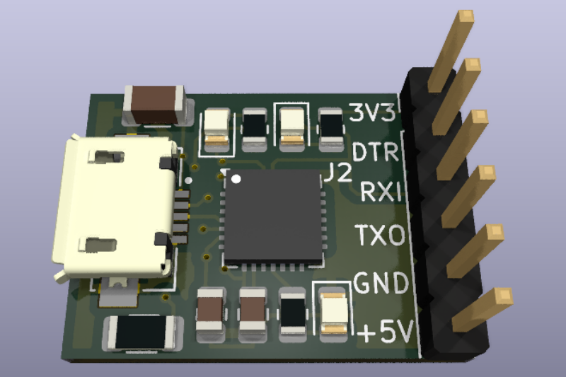
An open-source reverse-engineered version of the CJMCU CP2102 USB to UART TTL adapter, based on the original component available here. This project aims to provide insights into USB-to-serial communication and offer a customizable alternative for embedded system developers.
| Feature | Original Module | Reverse-Engineered Version |
|---|---|---|
| 🖥️ PCB Design | Proprietary | Open-source & customizable |
| 🔌 USB Connector | Micro USB | Micro USB |
| 🏷️ Chipset | CP2102 | CP2102 |
| 📌 Pin Mapping | 6-Pin UART TTL | 6-Pin UART TTL |
| ⚡ Supported Voltage | 3.3V / 5V | 3.3V / 5V |
| 👐 Mechanical Drawing | 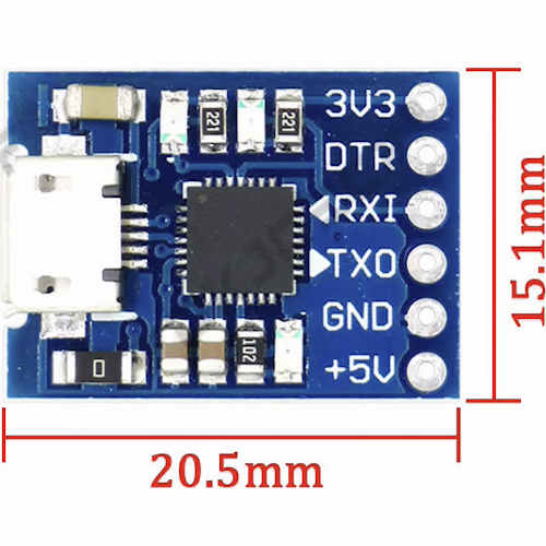 | 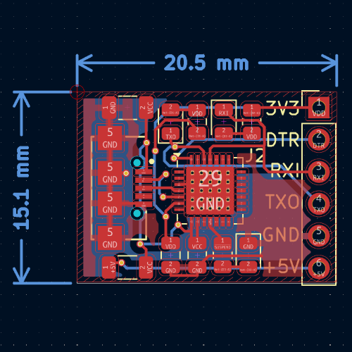 |
| 📝 Reverse-Engineered Schematic | N/A | 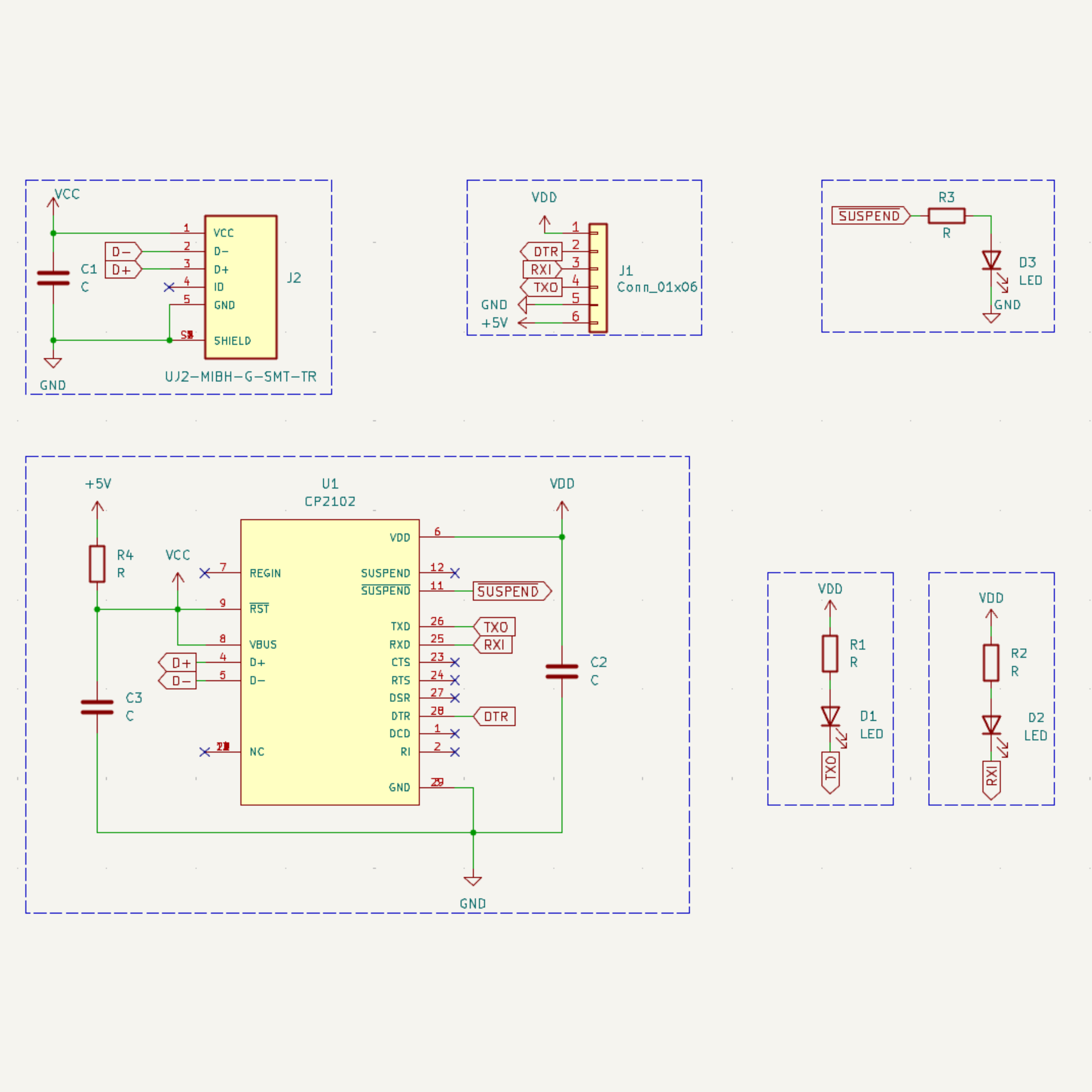 |
| 📷 Photo | 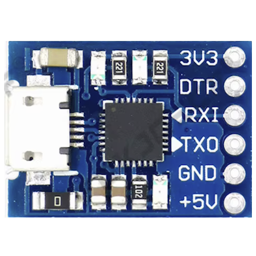 | 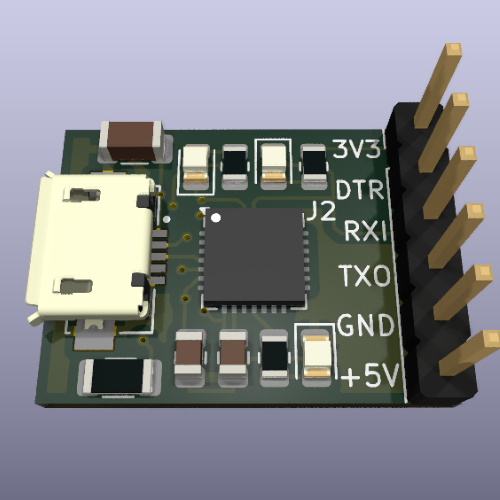 |
| CP2102 Pin | Description |
|---|---|
| TXD | Transmit Data |
| RXD | Receive Data |
| GND | Ground |
| 3V3 | 3.3V Power Output |
| 5V | 5V Power Output |
| DTR | Data Terminal Ready |
This project is open-source. Feel free to use, modify, and contribute! 🚀
| Qty | Value | Footprint | References |
|---|---|---|---|
| 3 | LED | LED_SMD:LED_0805_2012Metric | D1, D2, D3 |
| 3 | R | Resistor_SMD:R_0805_2012Metric | R1, R2, R3 |
| 2 | C | Capacitor_SMD:C_0805_2012Metric | C2, C3 |
| 1 | C | Capacitor_SMD:C_1206_3216Metric | C1 |
| 1 | CP2102 | Package_DFN_QFN:QFN-28-1EP_5x5mm_P0.5mm_EP3.75x3.75mm_ThermalVias | U1 |
| 1 | Conn_01x06 | Connector_PinHeader_2.54mm:PinHeader_1x06_P2.54mm_Vertical | J1 |
| 1 | R | Resistor_SMD:R_1206_3216Metric | R4 |
| 1 | UJ2-MIBH-G-SMT-TR | footprints:CUI_UJ2-MIBH-G-SMT-TR | J2 |
It measures 20.5 × 15.1 mm and has 2 copper layers, 1.6 mm thick.
13 parts, built around the CP2102 and UJ2-MIBH-G-SMT-TR. The full list of its parts is on this page, with links to each part's symbol and footprint where PCBKit's library has them.
From the mpek29/CP2102USB2UART repository on GitHub, at the commit this page was made from: the board is design/CP2102USB2UART/CP2102USB2UART.kicad_pcb and its schematic design/CP2102USB2UART/CP2102USB2UART.kicad_sch. PCBKit opens the board in the browser, with nothing to install.
Its repository states no licence, so its author keeps all rights: ask mpek29 before reusing the design.


abzman/esp-IoT-boards
R5v: 1.9K for the red LED, 3.9K for the blue LED

ExploreEmbedded/8051_DevelopmentBoard
Design files and sample code for 8051 development Ultra Boards

leafai-io/leaf-node-v3.x
Modular node for sensor monitoring and device control in grow environments.

ExploreEmbedded/hornbill-our
Open Univeral Remote with Hornbill ESP32 dev tools. BLE IR Bridge for device control

balmerdx/BalmerDX_VNA
Vector Network Analyzer 10 KHz - 180 MHz