2 layers30 × 52.5 mm

 mkovero/dbfob
Dirt-cheap keyfob noise-level indicator
Dbfob is an open-source printed circuit board by mkovero, from the mkovero/dbfob repository on GitHub. It is a 2-layer board of 30 × 26 mm with 24 parts on 28 nets, routed with 297 tracks and 38 vias.
It is built around the CH32L103F8U6, NT3H2111W0FHKH and CC0603KRX7R9BB104, with the BS-08-B2AA001, IM66D130MV01XTMA1 and TS-1187A-B-A-B among its other parts. Its parts include 7 resistors, 6 capacitors, 4 diodes, 2 ICs and 1 connector.


30 × 38 mm, 2 layers. It answers one question before B1 is trusted: does B1's NFC antenna read on a phone with a CR2032 right behind it, and with what trim? This is experiment 4.
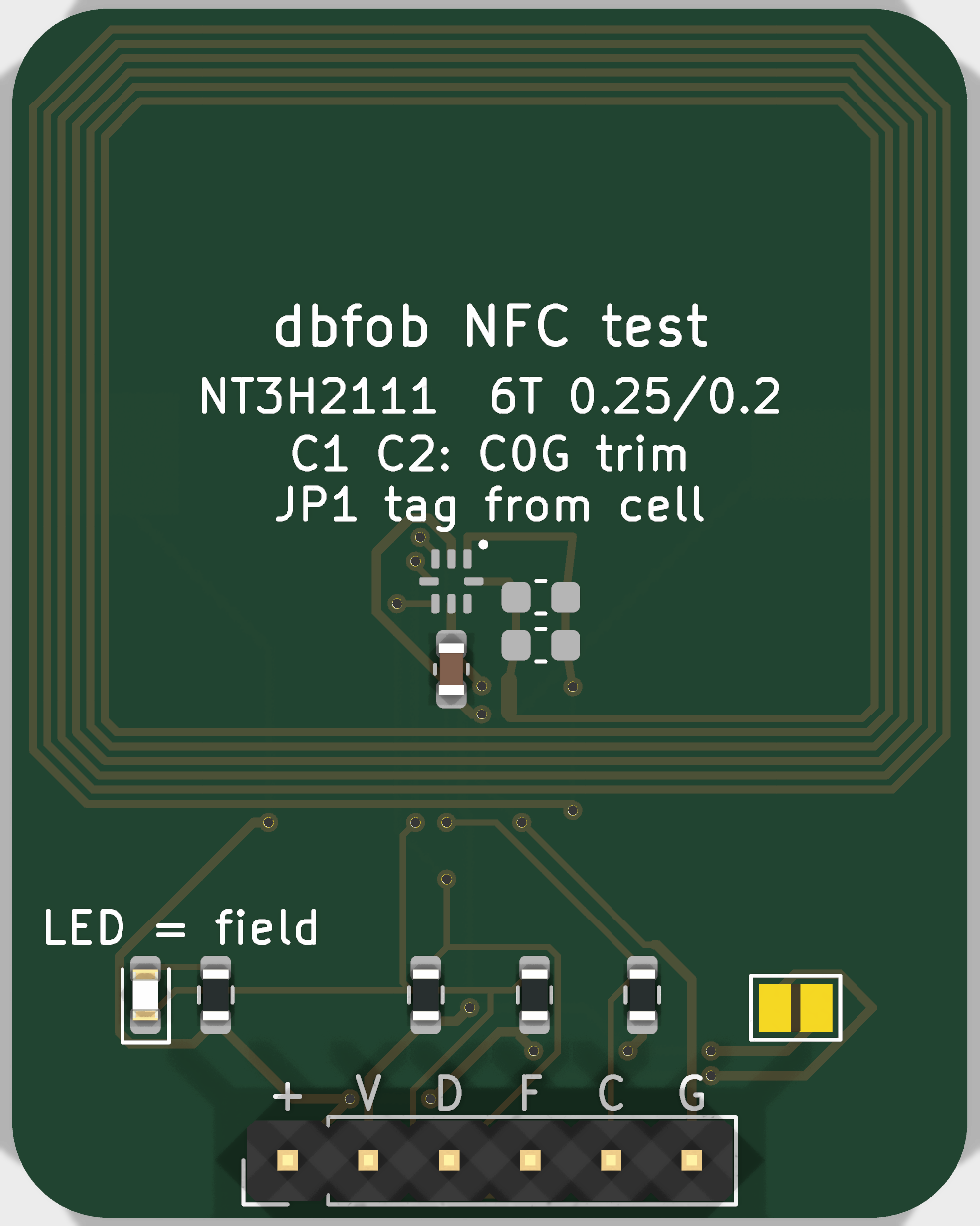
It goes in the same order as B1, so it can't steer B1's layout. B1 copies this antenna and its trim pads exactly. Whatever trim value this board finds goes straight onto B1's pads.
| Ref | What | Note |
|---|---|---|
| U1 | NT3H2111W0FHKH, C710403 | VOUT unused |
| C1, C2 | 0603 trim, not fitted | C0G, chosen on the bench |
| C3 | 100 nF | VCC decoupling |
| R1, R2 | 4.7 kΩ | SDA / SCL pull-ups to VCC |
| R3 | 10 kΩ | FD pull-up to the cell, as B1 will wake the MCU with it |
| R4, D1 | 1 kΩ, red | lit while a reader's field is on: FD pulls it low, even with VCC off |
| JP1 | solder jumper | bridge to run the tag's I2C side from the cell |
| BT1 | BS-08-B2AA001 (C964777) | hand-fit on the back, so JLC assembly stays one-sided |
| J1 | 1×6 2.54 mm, not fitted | + V D F C G = VBAT, VCC, SDA, FD, SCL, GND |
python3 hardware/lib/gen_lib.py               # NT3H2111 symbol, XQFN8 + BS-08 footprints
python3 hardware/nfc-test/tools/gen_sch.py    # tables -> schematic
python3 hardware/nfc-test/tools/make_pcb.py   # coil + placement + hand-drawn LA/LB, the router does the rest
python3 hardware/nfc-test/tools/fab.py        # -> production/
This follows the same procedure as rev A (../README.md).
How the antenna is drawn. The coil is LA track. Its inner end meets LB through net tie NT1; its outer end crosses under the turns on B.Cu (VO to VI) to reach the tag's LA pin. DRC doesn't check clearance within one net, so antenna.py builds the turns at a fixed pitch and asserts the 0.2 mm gap, and the vias' gap to the turns, itself.
State at commit:
Record f0, the trim value, the read distance and the LED distance for each of steps 1, 3 and 4. The step 4 trim value goes on B1's pads.
Why the coil is under 2.75 µH. 13.56 MHz needs 2.75 µH with the tag's 50 pF (44–56 pF). The coil is short of that on purpose: ferrite raises L, the cell lowers it, and a parallel trim cap can only pull the resonance down.
| Qty | Value | Footprint | References |
|---|---|---|---|
| 3 | 2.2k | Resistor_SMD:R_0603_1608Metric | R5, R6, R7 |
| 2 | 100n | Capacitor_SMD:C_0603_1608Metric | C3, C4 |
| 2 | 4.7k | Resistor_SMD:R_0603_1608Metric | R1, R2 |
| 2 | tune C0G | Capacitor_SMD:C_0603_1608Metric | C1, C2 |
| 1 | 100k | Resistor_SMD:R_0603_1608Metric | R3 |
| 1 | 10u | Capacitor_SMD:C_0603_1608Metric | C5 |
| 1 | 1k | Resistor_SMD:R_0603_1608Metric | R4 |
| 1 | 1u | Capacitor_SMD:C_0603_1608Metric | C6 |
| 1 | CH32L103F8U6 | Package_DFN_QFN:UQFN-20-1EP_3x3mm_P0.4mm_EP1.85x1.85mm | U2 |
| 1 | CR2032 | dbfob:BatteryHolder_MYOUNG_BS-08-B2AA001_CR2032 | BT1 |
| 1 | IM66D130M | dbfob:Infineon_IM66D130M_LGA-5_3x2mm | MK1 |
| 1 | NT3H2111W0FHK | dbfob:NXP_XQFN-8_1.6x1.6mm_P0.5mm | U1 |
| 1 | PROG | dbfob:TestPads_1x05_P2.54mm_D1.2mm | J1 |
| 1 | antenna | NetTie:NetTie-2_SMD_Pad0.5mm | NT1 |
| 1 | measure | Button_Switch_SMD:SW_Push_1P1T_XKB_TS-1187A | SW1 |
| 1 | orange 605nm | LED_SMD:LED_0603_1608Metric | D3 |
| 1 | red 625nm | LED_SMD:LED_0603_1608Metric | D4 |
| 1 | yellow 590nm | LED_SMD:LED_0603_1608Metric | D2 |
| 1 | yellow-green 575nm | LED_SMD:LED_0603_1608Metric | D1 |
It measures 30 × 26 mm and has 2 copper layers, 1.6 mm thick.
24 parts, built around the CH32L103F8U6, NT3H2111W0FHKH, CC0603KRX7R9BB104 and BS-08-B2AA001. The full list of its parts is on this page, with links to each part's symbol and footprint where PCBKit's library has them.
From the mkovero/dbfob repository on GitHub, at the commit this page was made from: the board is hardware/b1/b1.kicad_pcb and its schematic hardware/b1/b1.kicad_sch. PCBKit opens the board in the browser, with nothing to install.
Its repository states no licence, so its author keeps all rights: ask mkovero before reusing the design.


slemanz/chronolog
STM32-based temperature data logger with RTC, NOR flash storage, LCD and Wi-Fi. Hardware and firmware.

HeyPCB/badge-blob
Blob, the social battery badge: The name badge that tells people whether to come say hi. KiCad 10, heypcb.ai merch.

ilomon10/embedded-totalizer-hour-meter
ESP32 engine hour meter & totalizer: firmware, SensorFrame protocol, Node host tools, KiCad PCB and a Deno device simulator

tsmiltonAgents/20260721_countdown
A 46 × 23 mm, 4-layer keyring PCB that counts down the hours to 10 October 2026, midday on a red 4-digit 7-segment display.

soldernerd/InclinationMeter
A battery-powered, Bluetooth-enabled precision electronic level instrument for machine tool geometry inspection and granite surface plate qualification.

ThatguyCplus/throttleECU
STM32F411CE Throttle ECU — PID position control with AS5048A encoder, H-bridge motor, safety module

HeyPCB/cable-bunny
Cable Bunny: Is it a charge-only cable? Ask the bunny. KiCad 10, heypcb.ai merch.

robertxdx/ESP32S3PD15W
A 15 W USB-C powered ESP32-S3 LED-strip controller and development board.