4 layers47 × 47 mm
Motor Gen2
RoMeLaUCLA/romela-motor-driver
Motor driver PCB and firmware designed for RoMeLa actuators.
151 parts6MIT
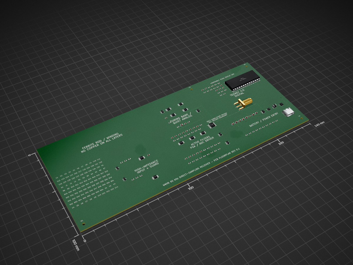
 McNeight/WWVB_AI
This directory contains the initial native KiCad project for the 60 kHz direct-sampling WWVB receiver:
WWVB Receiver is an open-source printed circuit board by McNeight, from the McNeight/WWVB_AI repository on GitHub, published under the MIT licence. It is a 4-layer board of 240 × 100 mm with 114 parts on 131 nets, routed with 87 tracks and 39 vias.
It is built around the OPA2320, BQ24074RGTR and BAV199. Its parts include 55 resistors, 31 capacitors, 11 ICs, 2 diodes and 1 connector.


This directory contains the initial native KiCad project for the 60 kHz direct-sampling WWVB receiver:
WWVB_Receiver.kicad_sch defines the native KiCad project-level interface-net contract.WWVB_Receiver.kicad_pcb is a four-layer placement floorplan. Its antenna zone is a real all-copper-layer keepout.This is an architecture capture, not a released schematic. The ferrite resonator's nominal 4.7 mH and 1.50 nF C0G-plus-trim values are retained. The following decisions must be closed before capture proceeds into routable circuitry:
The resonator is a floating, parallel tank: the nominal 4.7 mH ferrite winding and 1.50 nF C0G-plus-trim capacitor connect only between ANT_H and ANT_LO. Neither terminal may be connected directly to VMID, AGND, a shield, or a clamp rail.
ANT_H and ANT_LO each feed a separate, unity-gain non-inverting buffer through a preliminary 4.7 kOhm series protection resistor. A matched 10 MOhm resistor from each buffer input to VMID establishes its DC common-mode voltage while presenting a nominal 20 MOhm differential load to the tank. The two buffer outputs are the differential signal pair presented to the subtractor/first active-filter stage. This preserves the tank's differential signal, limits common-mode conversion, and keeps the low-impedance filter network from loading its resonant resistance.
Use the two channels of an OPA2320 in a VSSOP-8 package for these buffers; it is specified for 1.8 V to 5.5 V operation, has 7 nV/root-Hz input voltage-noise density, 1.45 mA typical quiescent current per channel, rail-inclusive input common-mode range, and near-rail output swing. The previously proposed OPA1655 is rejected for this receiver because its 4.5 V minimum supply and 3.9 mA supply current do not meet the 3.3 V low-power constraint.
Use one Nexperia BAV199 per buffer input. The BAV199 is a low-leakage dual diode in a SOT-23 package, connected in series internally: pin 3 is the shared cathode of diode 1 and anode of diode 2. Connect pin 3 to CLAMP_P or CLAMP_N, pin 1 to AGND, and pin 2 to AVDD_3V3. This creates the required rail clamp: negative excursions forward-bias the AGND-to-clamp diode and positive excursions forward-bias the clamp-to-AVDD_3V3 diode.
For each tank terminal, use this sequence:
ANT_H or ANT_LO -> 4.7 kOhm (RPROT) -> CLAMP_P or CLAMP_N -> 1.0 kOhm (RISO) -> OPA2320 non-inverting input.
The 10 MOhm input-bias resistor remains on the OPA2320 side of RISO. The BAV199 clamps are therefore isolated from the resonator by RPROT and from the OPA2320 internal rail-clamp diodes by RISO. Do not fit TVS diodes, Schottky diodes, or protection capacitors directly to ANT_H or ANT_LO.
At 60 kHz, the input network's resistor noise is approximately 13.7 nV/sqrt(Hz) differential for the two 5.7 kOhm paths. The two OPA2320 buffer channels add approximately 9.9 nV/sqrt(Hz) differential, giving about 17 nV/sqrt(Hz) combined before tank and atmospheric noise. This remains below the approximately 34 nV/sqrt(Hz) thermal noise of a 70 kOhm resonant source resistance. The BAV199's 3 pA typical reverse leakage and 2 pF typical capacitance are acceptable only because it is placed after RPROT; tune the final tank with all populated input-protection parts installed.
The BAV199 pulse rating does not establish IEC 61000-4-2 compliance for an exposed antenna port. This receiver has an on-board, enclosed ferrite winding; if a remote or user-accessible antenna is added, it requires a separate connector-level IEC protection design and requalification.
Use one OPA320 as a unity-gain differential subtractor between BUF_P/BUF_N and the high-pass/active-filter chain. Implement the four gain-defining resistors with one LT5400-1 matched quad 10.0 kOhm network: connect BUF_N through R1 to the OPA320 inverting input, OPA320 output through R2 to the inverting input, BUF_P through R3 to the non-inverting input, and VMID_AC through R4 to the non-inverting input. With the matched unity ratios, DIFF_OUT = VMID_AC + BUF_P - BUF_N.
The LT5400-1's 0.01% maximum resistor-ratio error and 2 ppm/degree C ratio tracking preserve differential common-mode rejection far better than separately sourced 0.1% resistors. Keep the resistor network and OPA320 adjacent in the quiet-analog zone, route BUF_P and BUF_N as a short symmetric pair, and keep DIFF_OUT on Layer 1 over the continuous AGND plane. Do not add a feedback capacitor across the subtractor; the dedicated 89.4 kHz anti-alias filter provides the required post-subtraction bandwidth limit.
The previously proposed ADG704 is not retained. It is a 1:4 analog multiplexer/demultiplexer, rather than a bank of independently controlled SPST switches, and does not provide enough gain states for the intended acquisition-to-tracking range.
Use a TMUX1208PWR 8:1 analog multiplexer with AVDD_3V3 and AGND supplies. It is a production 16-pin TSSOP device specified for a 1.08 V to 5.5 V supply, rail-to-rail signal range, 1.8 V-compatible logic thresholds, break-before-make switching, and 9 Ohm typical on-resistance at 3.3 V (17 Ohm maximum over temperature). Its 3.3 V maximum supply current is 1.5 uA. The mux is downstream of the resonator buffers and active filters, so its leakage and capacitance do not load the tank.
Configure the PGA as an inverting OPA320 stage with its non-inverting input at VMID and a fixed 20.0 kOhm, 0.1% feedback resistor. Connect BPF2_OUT to each TMUX1208 Sx pin through one 0.1% input resistor; connect the TMUX1208 drain to the OPA320 inverting input. The firmware selects one path at a time:
| Selected channel | Input resistor | Nominal voltage gain |
|---|---|---|
| S1 | 160 kOhm | -0.125 V/V |
| S2 | 80.6 kOhm | -0.248 V/V |
| S3 | 40.2 kOhm | -0.498 V/V |
| S4 | 20.0 kOhm | -1.00 V/V |
| S5 | 10.0 kOhm | -2.00 V/V |
| S6 | 4.99 kOhm | -4.01 V/V |
| S7 | 2.49 kOhm | -8.03 V/V |
| S8 | 1.24 kOhm | -16.1 V/V |
AGC_MUX_A0, AGC_MUX_A1, and AGC_MUX_A2 each have a 100 kOhm pull-down to AGND; AGC_MUX_EN has a 100 kOhm pull-down and enables the mux only after firmware configures a valid channel address. A disabled mux leaves the fixed OPA320 feedback path intact and holds the PGA output at VMID, rather than allowing an open-loop amplifier condition. Firmware must deassert AGC_MUX_EN, change the address, wait at least 1 us, then assert AGC_MUX_EN.
The listed gain values exclude the mux on-resistance. The 9 Ohm typical resistance produces less than 0.8% gain error for S8, and the high-gain states must be calibrated with the receiver's injected calibration signal before reporting amplitude metrics.
At 60 kHz, the high-pass plus low-pass chain gain is 2.525 V/V and the subtractor gain is unity. The complete analog gain from DIFF_OUT to ADC_IN is therefore 0.316 V/V through 40.72 V/V, or -10.02 dB through 32.20 dB, across the eight PGA states. A 1.10 V peak ADC swing corresponds to DIFF_OUT peaks of 3.486 V, 1.756 V, 875.8 mV, 435.7 mV, 217.9 mV, 108.7 mV, 54.3 mV, and 27.0 mV respectively from S1 through S8.
The ADC driver is centered at 1.65 V. Normal tracking targets a 0.80 V peak carrier excursion, or a 0.85 V to 2.45 V signal range. A block peak beyond 1.15 V from VMID_AC is an immediate fast-attack condition: disable the TMUX1208, select the next lower gain, wait 1 ms, enable the selected path, and invalidate the affected DSP block. A block peak beyond 1.30 V is an overload fault; step directly to S1 and restart acquisition.
Increase gain only after at least 1 second of uninterrupted tracking when the 99th-percentile carrier peak is below 0.15 V from VMID_AC and no overload or AGC transition occurred. Gain changes are permitted only between decoded seconds; the receiver records the selected gain and calibrated gain correction with every signal-quality measurement. The Costas loop and envelope estimator discard at least 10 ms after every gain transition.
The ferrite resonator supplies the high-Q portion of the analog bandpass. A separately tuned, high-Q active MFB filter is rejected because it adds excessive frequency and Q sensitivity without providing useful selectivity beyond the measured resonator response. The active chain instead uses a DC-blocking high-pass section followed by a fourth-order Butterworth low-pass filter. Together with the loaded ferrite tank, this produces the required 60 kHz system bandpass while preserving tolerance margin and stable gain.
After the differential subtractor, place a 10 nF C0G coupling capacitor in series with the signal and a 3.92 kOhm, 0.1% resistor from its output to VMID. This 4.06 kHz first-order high-pass section rejects residual low-frequency interference and removes buffer/subtractor offset without materially attenuating 60 kHz.
The anti-alias filter is two cascaded, non-inverting Sallen-Key low-pass stages implemented with an OPA2320. Each uses 1.78 kOhm, 0.1% resistors and 1.00 nF, 1% C0G capacitors, setting a nominal 89.4 kHz pole frequency. Connect the lower-Q stage first:
| Stage | R1, R2 | C1, C2 | Gain resistor to VMID | Feedback resistor | Gain | Q |
|---|---|---|---|---|---|---|
| LP1 | 1.78 kOhm | 1.00 nF | 10.0 kOhm | 1.50 kOhm | 1.150 V/V | 0.541 |
| LP2 | 1.78 kOhm | 1.00 nF | 10.0 kOhm | 12.4 kOhm | 2.240 V/V | 1.316 |
For each Sallen-Key stage, use the standard low-pass connection: R1 from input to the RC junction, R2 from the RC junction to the non-inverting input, C1 from the non-inverting input to VMID, and C2 from the RC junction to the op-amp output. The gain-setting resistors connect from the inverting input to VMID and from the output to the inverting input. The combined nominal gain at 60 kHz is 2.525 V/V (8.04 dB).
Relative to the 60 kHz response, this active chain attenuates 60 Hz by 36.4 dB, 240 kHz by 34.1 dB, 420 kHz by 53.6 dB, 500 kHz by 59.6 dB, and 1 MHz by 83.7 dB. The resonant antenna adds substantial rejection outside its approximately 600 Hz to 1000 Hz loaded passband. With independent 0.1% resistor and 1% capacitor variation, a 5,000-run tolerance analysis predicts 60 kHz gain from 7.91 dB to 8.18 dB for the central 90% of builds; calibration removes this gain spread.
Connect ADC_IN to Teensy 4.0 pin 16 / A2, which is ADC2 channel 12. This pin is dedicated to the receiver; do not attach a digital peripheral, LED, or test fixture that can inject switching noise. The OPA320 ADC driver is unity gain and biased at VMID. Place a 47 Ohm resistor directly at the OPA320 output and a 470 pF C0G capacitor from the Teensy side of that resistor to AGND; this isolates the driver from the ADC sampling transient without changing the 60 kHz or analog anti-alias response.
Build firmware for a 240 MHz CPU clock. The PJRC clock configuration gives this setting a 120 MHz IPG bus clock. Configure QTMR4 channel 3 to toggle its output every 125 IPG clocks, producing an exact 480,000 samples/s trigger. Route XBARA1_IN_QTIMER4_TIMER3 to XBARA1_OUT_ADC_ETC_TRIG00 + 4, configure ADC_ETC trigger 4 for one ADC2 conversion, and take data from IMXRT_ADC_ETC.TRIG[4].RESULT_1_0. Configure the DMA channel to use DMAMUX_SOURCE_ADC_ETC; no sample-rate ISR or polling is permitted.
Configure ADC2 for a single externally triggered 12-bit conversion: external trigger enabled, high-speed conversion enabled, IPG clock divided by four, long sample mode disabled, and hardware averaging disabled. This produces a 30 MHz ADC conversion clock, within the 40 MHz high-speed limit used by the PJRC ADC implementation, while preserving the 480 ksample/s sampling interval for digital oversampling. The raw source impedance is the low-impedance OPA320 driver rather than the resonator or active-filter network.
Use four 1,920-sample, 16-bit DMA blocks in DMA-accessible OCRAM, each aligned to a 32-byte cache line. A block contains 4.00 ms of raw data and is exactly divisible by the decimation factors of 10 and 12. Invalidate its data-cache lines before DSP consumption, maintain a producer/consumer index, and treat a producer overrun as a receiver fault that resets acquisition rather than silently discarding data.
The 480 ksample/s to 4 ksample/s decimation ratio is 120, which provides 20.8 dB of white-noise processing gain (3.45 ideal ENOB-equivalent bits) before the envelope and carrier loops. Actual ADC ENOB must be characterized with a terminated input; the Teensy documentation cautions that only about 10 bits are commonly usable from simple analogRead use, so the receiver must not claim a 12-bit noise floor without measurement.
Use one OPA320 as a unity-gain non-inverting voltage follower between VGA_OUT and the Teensy ADC input. Its non-inverting input connects directly to VGA_OUT; its inverting input connects directly to its output. The output remains biased at VMID_AC and requires no coupling capacitor or level-shift stage.
Place a 47 Ohm, 0.1% resistor in series at the OPA320 output. On the Teensy side of this resistor, place a 470 pF C0G capacitor to AGND and route the resulting net as ADC_IN directly to Teensy pin 16 / A2. This network has a nominal 7.21 MHz pole, isolates the OPA320 from ADC sampling-current transients, and is electrically insignificant at 60 kHz. The 470 pF capacitor return must use the same short AGND path as the OPA320 bypass capacitor; it must not return through DGND or the Teensy digital ground plane.
Do not add a clamp, pull resistor, jumper, RC filter, or test point on the Teensy side of the 47 Ohm resistor. Any protection of ADC_IN is provided by the OPA320's bounded output swing and the PGA fast-attack policy. If a test pad is required, place it only on VGA_OUT, before the ADC driver, with its adjacent AGND reference pad.
Route ADC_IN only on Layer 1 from the 47 Ohm resistor to Teensy pin 16 / A2, with a maximum physical trace length of 30 mm and no vias. The trace stays over uninterrupted AGND until the single designated AGND/DGND bridge at the Teensy analog-input boundary. The KiCad custom rules file enforces the 30 mm maximum length and 0.3 mm clearance once the net is imported from the populated schematic.
The released analog stages use approximately 10.15 mA typical before the VMID buffer, regulators, Teensy 4.0, and conversion/DMA/DSP load: 2.90 mA for the OPA2320 input buffers, 1.45 mA for the differential subtractor, 2.90 mA for the OPA2320 low-pass pair, 1.45 mA for the PGA, and 1.45 mA for the ADC driver. This leaves less than 4.85 mA for all remaining functions under the 15 mA target. A continuously sampling Teensy 4.0 cannot be assumed to fit this remainder, even at 240 MHz.
The 15 mA target is therefore retired for the retained Teensy architecture. Measure complete-board current with the specified 480 ksample/s DMA and DSP workload before quoting a consumption figure. Continuous BPSK phase tracking remains a required function and must not be disabled to reduce a published power value.
The production power figure must be established at the regulated 3.3 V input with USB disconnected, all released analog stages populated, the CPU at 240 MHz, ADC2/DMA running at 480,000 samples/s, the carrier loop locked, the envelope path active, and quality telemetry enabled. Record the 60-second average, 95th-percentile current, and maximum observed current during a WWVB frame boundary and AGC transition. Separately record battery-input current and converter efficiency for the intended battery-voltage range; do not substitute that figure for the regulated-rail operating current.
Use a protected, single-cell 1200 mAh to 2000 mAh Li-ion/LiPo pack and configure the BQ24074 power-path charger for 500 mA charging from a power-only USB-C receptacle. The USB-C receptacle uses 5.1 kOhm pull-down resistors on CC1 and CC2 and does not carry data. Set EN1 high and EN2 low for USB500 input-current mode, and connect a 1.78 kOhm, 1% resistor from ISET to VSS; the BQ24074 K_ISET nominal value of 890 A gives 500 mA nominal fast-charge current. Dynamic power-path management reduces battery charge current whenever the system load consumes part of the 500 mA USB budget. Connect the pack's 10 kOhm NTC to TS; do not bypass temperature monitoring. Connect a 46.4 kOhm, 1% resistor from TMR to VSS for a nominal 6.25-hour fast-charge safety timer. Leave ITERM intentionally unconnected to select the BQ24074's default 10% termination threshold, or 50 mA at the configured 500 mA charge current. Tie CE to VSS through 10 kOhm so charging is enabled before firmware starts. Pull the open-drain CHG and PGOOD outputs up to DVDD_3V3 with 47 kOhm resistors and route them through the TEENSY_DSP sheet as status-only inputs. The BQ24074 OUT power-path node supplies the remainder of the receiver while the battery charges.
Use an adjustable TPS63030 buck-boost converter to generate a 3.60 V preregulator rail, VPREREG_3V6, across the protected battery discharge range. The TPS63030 feedback reference is 500 mV, not 1.20 V. Set its feedback divider to 1.24 MOhm from VOUT to FB and 200 kOhm from FB to GND; this implements VOUT = 0.5 V x (1 + R1/R2) = 3.60 V and follows the data-sheet recommendation to use an approximately 200 kOhm lower divider resistor. Use a 1.5 uH shielded inductor, a 10 uF X7R input capacitor, two 10 uF X7R output capacitors, and a 100 nF X7R local bypass capacitor as the documented baseline power stage. Tie PS/SYNC high to disable power-save mode and force fixed-frequency PWM operation during receive, avoiding low-frequency pulse bursts. Locate the complete switching loop in the power-entry zone, at the opposite board edge from the ferrite rod. VPREREG_3V6 feeds Teensy 4.0 VIN, allowing the module's onboard regulator to generate DVDD_3V3. Do not inject an external 3.3 V supply into the Teensy 3.3 V pad or its USB-VBUS path.
Generate AVDD_3V3 from VPREREG_3V6 with a TPS7A2033 low-noise 300 mA LDO. Fit 4.7 uF X7R capacitors at both its input and output; these exceed the 1 uF minimum stability requirement and are placed at the regulator pins. The analog LDO is the only supply source for the OPA2320/OPA320 stages, TMUX1208, and the reference buffer; no digital load may share its output trace. Connect AGND and DGND only at the intentional ADC/reference boundary.
Generate VMID with a matched 10.0 kOhm, 0.1% divider from AVDD_3V3 to AGND, bypass it with 10 uF plus 100 nF to AGND, and buffer it with a unity-gain OPA320. VMID_AC is the buffer output and serves as the local AC reference for the filters and PGA. It is not a system ground, a ferrite return, or a clamp-current return.
USB charging is a maintenance mode, not a low-noise receive mode. The published sensitivity and power measurements require the USB-C cable to be disconnected. The BQ24074, TPS63030, LDOs, USB-C connector, inductor, and their high-current capacitors belong only in the power-entry PCB zone; no switching node, charger trace, or VPREREG_3V6 copper may enter the antenna or high-impedance input zones.
Replace the nominal single 1.50 nF tank capacitor with a fixed C0G/NP0 parallel capacitor bank connected directly across ANT_H and ANT_LO. Fit the 1.00 nF, 50 V C0G base capacitor. Provide independent 0603 footprints for 470 pF, 220 pF, 100 pF, 47 pF, 22 pF, 10 pF, and 4.7 pF C0G capacitors; install only the values needed after measurement. This gives a populated external range from 1.000 nF to 1.874 nF in a minimum 4.7 pF step, while avoiding a variable capacitor's temperature coefficient, mechanical drift, and microphonic behavior.
For the nominal 4.7 mH winding, the 60 kHz total capacitance is 1.497 nF. A measured 97 pF distributed/input capacitance therefore calls for approximately 1.400 nF of fitted capacitor-bank capacitance: 1.00 nF + 220 pF + 100 pF + 47 pF + 22 pF + 10 pF. The bank has sufficient range for winding inductance from approximately 3.75 mH through 7.04 mH before accounting for distributed capacitance. It is not a substitute for measuring the actual winding at 60 kHz.
Tune only with the OPA2320 input buffers, BAV199 clamps, the intended enclosure, and all final nearby hardware installed. Drive a separate calibrated magnetic coupling loop with a swept, low-level source; observe the differential buffered output, not the bare tank with a probe. Determine distributed capacitance from two capacitor/resonance measurements, calculate the initial bank population, then select the final 4.7 pF to 22 pF increments for a 60.000 kHz peak. Record the populated values, 3 dB frequencies, loaded Q, and resonant resistance in the unit calibration record.
Do not fit a trimmer, scope test pad, jumper, TVS, or copper pour directly to either tank terminal. The capacitor-bank components and their traces remain inside the antenna no-copper region and are the only intentional components connected across the resonator.
Use a 1.60 mm four-layer FR-4 board with 1 oz outer copper and at least 0.5 oz inner copper. Layer 1 is for components and short critical analog routes. Layer 2 is a continuous AGND reference plane throughout the quiet analog region. Layer 3 distributes VPREREG_3V6, AVDD_3V3, and battery/charger power in the power zone and forms the DGND reference plane beneath the Teensy. Layer 4 carries low-speed digital control and noncritical return routes. No copper, plane, via, pad, footprint, or routing is allowed on any layer within the ferrite rod/winding keepout.
Maintain AGND and DGND as separate copper regions. They join at one short, intentional connection adjacent to the ADC driver/Teensy analog-input boundary. The ADC driver output and its 470 pF capacitor use AGND locally; the connection to Teensy A2 crosses to the digital region only at this designated bridge. Do not place a split, slot, or plane void beneath this routed input or its local return path.
The differential antenna buffer pair occupies the high-impedance zone directly below the rod's winding center, beginning at least 15 mm beyond the ferrite no-copper boundary. The subtractor, high-pass network, Sallen-Key filters, PGA, ADC driver, VMID buffer, and their decoupling capacitors occupy the adjacent quiet-analog zone. All analog circuitry is on Layer 1 over uninterrupted Layer 2 AGND. Keep each 100 nF analog bypass capacitor at its IC power pins with a dedicated, adjacent Layer 2 via. The BQ24074, TPS63030, inductor, input/output capacitors, USB-C connector, and battery connections occupy the power-entry zone only. Keep their high di/dt loops entirely on Layer 1 and Layer 3 and outside the analog plane region.
Route AGC_MUX_A0, AGC_MUX_A1, AGC_MUX_A2, and AGC_MUX_EN on Layer 4. Each passes through a 1 kOhm series resistor at the digital-zone boundary and has no parallel run with ANT_H, ANT_LO, the differential buffer outputs, or ADC_IN. Use the Teensy’s lowest available drive strength and 50 MHz pad bandwidth for these controls.
VMID_AC policyFit one 100 nF, 25 V C0G capacitor from AVDD_3V3 to AGND at each OPA320 or OPA2320 package, with capacitor pads and the ground via closer to the IC supply pins than any other copper. Fit one additional 1.0 uF, 10 V X7R capacitor per analog functional cluster: input buffers, differential subtractor/high-pass, low-pass pair, PGA/ADC driver, and VMID_AC buffer. The TMUX1208 receives its own 100 nF C0G capacitor and shares the PGA/ADC-driver 1.0 uF bulk capacitor.
Generate the unbuffered VMID divider node with the matched 10.0 kOhm resistors, a 10 uF X7R capacitor, and a 100 nF C0G capacitor to AGND. Route this node only to the OPA320 reference-buffer input. VMID_AC, the buffer output, is the only reference net permitted to reach the subtractor, high-pass bias resistor, Sallen-Key capacitors/gain networks, PGA non-inverting input, and input guards. Keep the buffer output trace short and branch it as a star from the buffer; do not daisy-chain it through the signal path.
Do not place a ferrite bead, series resistor, switching rail, or digital decoupling return in the AVDD_3V3 path between the TPS7A2033 output capacitor and the analog functional clusters. The LDO and local capacitors provide the low-noise source. All analog bypass and VMID_AC capacitor returns use AGND vias only; no such capacitor may return to DGND.
Do not place a conductive shield around, beneath, or within 15 mm of the ferrite rod or its winding. At 60 kHz, copper or other closed conductive paths near the rod support eddy currents that lower resonator Q and reduce magnetic sensitivity. The all-layer antenna keepout is therefore the primary antenna shield policy, not an omitted ground plane.
Guard only the two OPA2320 buffer input nodes after their 4.7 kOhm RPROT resistors. Route a narrow VMID_AC guard trace on Layer 1 around the CLAMP_P/CLAMP_N to buffer-input segments, with no Layer 2 guard plane beneath the ferrite or tank terminals. The guard reduces leakage and capacitive pickup at the op-amp inputs without creating an AC return path across the resonator. Do not guard ANT_H or ANT_LO.
Fit a removable grounded metal or conductive-coated shield over the Teensy and power-entry zones only. Bond this shield to DGND at one point next to the power entry and keep it at least 65 mm from the ferrite rod keepout. Do not bond it to AGND, VMID, VMID_AC, or the ADC driver return. The shield should cover the Teensy, USB-C connector, BQ24074, TPS63030, and inductor, while leaving the quiet analog and ferrite zones uncovered.
Provide an optional DGND via fence along the digital side of the analog/digital boundary, beginning no closer than 15 mm from the high-impedance buffer input. The fence vias are 0.8 mm diameter with 0.4 mm drill on 5 mm pitch and must terminate at the boundary rather than extending toward the ferrite. This confines digital electric-field return currents without forming a loop around the antenna.
Use four non-plated 2.5 mm mounting holes at board coordinates H1 (25, 115), H2 (185, 25), H3 (255, 25), and H4 (255, 115), in millimeters relative to the PCB origin. Do not place plated mounting holes, conductive standoffs, screw heads, washers, or enclosure bosses within 15 mm of the ferrite rod/winding keepout or the tuning-bank components. H1 is intentionally below the antenna boundary; the other three mounting points are in the digital/power side of the board.
Use nylon standoffs and hardware for the enclosure around the ferrite, quiet-analog, and tuning-bank zones. Metal mounting hardware is permitted only in the digital/power region and must not contact AGND, DGND, or the removable shield can unless a later enclosure-grounding review explicitly approves it.
Use 0603 footprints for all fixed resistors and capacitors, including the tank capacitor bank, input protection, precision gain resistors, filters, and local bypassing. This package provides practical manual rework and measurement access without the parasitic area of 0805 parts. Do not substitute X7R dielectric for any tank, filter frequency-setting, or ADC-driver capacitor; these positions are 50 V C0G/NP0. The 1.0 uF through 10 uF supply-bulk positions are 10 V X7R 0603 or 0805 only where the required effective capacitance cannot be met in 0603.
Use VSSOP-8 for OPA2320, SOT-23-5 for OPA320 and TPS7A2033, SOT-23 for BAV199, TSSOP-16 for TMUX1208, VQFN-16 with exposed pad for BQ24074, and VSON-10 with exposed pad for TPS63030. Thermal pads use the library-recommended segmented paste stencil and multiple Layer 3 DGND/power-zone thermal vias only inside the power-entry zone. No exposed-pad thermal via, paste aperture, or large copper island is permitted in the antenna, high-impedance, or quiet-analog zones.
Use a fabrication process supporting 0.15 mm copper clearance at fine-pitch component pads and 0.20 mm minimum finished trace/space for all routed copper. Use a 0.30 mm finished mechanical drill for ordinary vias and 0.40 mm drill / 0.80 mm diameter for the DGND shield fence and power vias. The tank and high-impedance nets have no vias, as enforced by the project DRC rules. Place all component reference designators on F.SilkS outside the shield-can outline where they remain readable after assembly.
Use the installed KiCad symbols Battery_Management:BQ24074RGT, Regulator_Switching:TPS63030DSK, Regulator_Linear:TPS7A20xxxDBV, and Analog_Switch:TMUX1208PW with their manufacturer-matched package footprints. The BQ24074 uses the 3 mm x 3 mm 16-pin VQFN exposed-pad footprint, the TPS63030 uses the 3 mm x 3 mm 10-pin VSON exposed-pad footprint, the TPS7A2033 uses SOT-23-5, and the TMUX1208PWR uses the 16-pin 4.4 mm x 5 mm TSSOP footprint.
KiCad does not provide dedicated OPA320 or OPA2320 symbols. Use Amplifier_Operational:LM321 as the pin-compatible single-amplifier symbol for OPA320 devices and Amplifier_Operational:LM358 as the pin-compatible dual-amplifier symbol for OPA2320 devices. In each placed symbol, set Value to the actual OPA part number, set Manufacturer to Texas Instruments, assign the actual data-sheet URL, and attach the correct package footprint: SOT-23-5 for OPA320 and 3 mm x 3 mm, 0.65 mm-pitch VSSOP-8 for OPA2320.
Use Diode:BAV99 as the pin-compatible dual-series schematic symbol for the Nexperia BAV199, overriding Value to BAV199, the data sheet to the Nexperia BAV199 data sheet, and the footprint to Package_TO_SOT_SMD:SOT-23. Do not use KiCad's BAV199DW symbol: it represents a different four-diode SOT-363 device and would produce an incorrect pinout and footprint.
Reserve Teensy 4.0 pin 16 / A2 exclusively for ADC_IN and ADC2 channel 12. It has no digital peripheral, LED, pull resistor, test header, or shared function.
| Teensy pin | Net | Direction | Function |
|---|---|---|---|
| 2 | AGC_MUX_A0 | Output | TMUX1208 gain address bit 0 |
| 3 | AGC_MUX_A1 | Output | TMUX1208 gain address bit 1 |
| 4 | AGC_MUX_A2 | Output | TMUX1208 gain address bit 2 |
| 5 | AGC_MUX_EN | Output | TMUX1208 active-high enable |
| 6 | CAL_SELF_EN | Output | Onboard calibration-path enable |
| 7 | CAL_EXT_EN | Output | External calibration-path enable |
| 8 | CHG_N | Input | BQ24074 active-low charging status |
| 9 | PGOOD_N | Input | BQ24074 active-low input-power-good status |
| 10 | CAL_PWM | Output | 60 kHz self-test PWM source |
All outputs default to a high-impedance input during reset. The external 100 kOhm pull-down resistors on AGC_MUX_*, CAL_SELF_EN, and CAL_EXT_EN therefore establish the inactive hardware state before firmware executes. Route the AGC and calibration-enable signals through 1 kOhm series resistors at the digital-zone boundary. CHG_N and PGOOD_N are pulled up only to DVDD_3V3, then route through 1 kOhm series resistors to the Teensy inputs.
Firmware configures pins 2 through 7 and 10 for minimum drive strength and 50 MHz pad bandwidth. It configures pins 8 and 9 as inputs without internal pulls. Never use pins 0, 1, 13, 14, 15, 16, 17, 18, 19, 20, or 21 for this control interface; this preserves the USB/serial, onboard LED, dedicated ADC, and future I2C/SPI debug options.
Wind a separate three-turn AWG 32 enamelled-wire calibration coil over an 8 mm section at one end of the ferrite rod, outside the receive winding. This winding has no electrical connection to ANT_H or ANT_LO; it couples only magnetically. Route its twisted pair directly to the TEST_CALIBRATION sheet and keep it open-circuit whenever calibration is inactive.
Provide two independent, normally-off TMUX1101PWR analog-switch paths to the calibration coil. The external path is a dedicated SMA laboratory-input connector followed by a 1.0 kOhm source resistor and CAL_EXT_EN switch. The self-test path is a Teensy 60 kHz CAL_PWM output followed by a 1.0 kOhm source resistor and CAL_SELF_EN switch. Tie both switch outputs to CAL_SRC, then connect CAL_SRC through a 100 nF C0G DC-blocking capacitor and a final 1.0 kOhm resistor to CAL_COIL_P; CAL_COIL_N returns to AGND.
The TMUX1101 operates from DVDD_3V3/DGND, is normally open when its select input is low, accepts rail-to-rail 0 V to 3.3 V signals, and has 1.8 V-compatible control thresholds. Fit a 100 kOhm pull-down at each enable. Firmware may assert only one enable at a time; on boot, reset, normal receive, and before any AGC transition, both enables remain low. The AC-coupling capacitor prevents DC magnetization of the ferrite during PWM self-test.
The self-test PWM confirms signal-chain continuity and repeatable relative gain; it does not establish an absolute magnetic field. Absolute sensitivity and resonator measurements use the external source and a calibrated coupling fixture. The SMA shell and self-test driver return only to DGND in the digital/power zone, and the analog switches remain physically outside the ferrite and high-impedance input zones.
Do not place a test point, connector, jumper, via stub, or probe pad on ANT_H, ANT_LO, CLAMP_P, CLAMP_N, or either OPA2320 non-inverting input. Resonator frequency, Q, and resonant resistance are measured through the differential buffered outputs only.
Provide 1 mm signal pads and an adjacent 1 mm AGND reference pad for BUF_P, BUF_N, DIFF_OUT, HP_OUT, BPF1_OUT, BPF2_OUT, VGA_OUT, and the ADC-driver side of the 47 Ohm resistor. The signal/reference pairs are spaced 2.54 mm apart and oriented for a short differential probe or miniature coax probe. Keep each pad pair outside the ferrite keepout and at least 15 mm from the rod/winding boundary.
Provide 1 mm power/reference pads for VBAT, VPREREG_3V6, AVDD_3V3, DVDD_3V3, VMID_AC, AGND, and DGND. The VMID_AC pad must be adjacent to AGND only; it is not referenced to DGND. Place battery and preregulator pads in the power-entry zone, analog pads in the quiet-analog zone, and digital pads inside the shield-can zone.
Route no permanent oscilloscope ground lead across the antenna region. Use a differential probe for BUF_P to BUF_N and for any measurement that bridges AGND/DGND; use a short spring ground for single-ended analog measurements. All test pads are excluded from normal receive interconnects and exist only as compact copper landing pads.
The wwvbant.pdf reference reinforces that the resonator must be characterized at 60 kHz, not inferred from a 1 kHz inductance result. Before selecting the capacitor-bank population, measure distributed capacitance using two known capacitors and two resonance measurements, then measure loaded Q and resonant resistance after the intended buffer is attached.
Do not manufacture or route this revision.
| Qty | Value | Footprint | References |
|---|---|---|---|
| 12 | 1k | Resistor_SMD:R_0603_1608Metric | R42, R43, R44, R45, R46, R47, R48, R49, R50, R51, R52, R53 |
| 6 | 100k | Resistor_SMD:R_0603_1608Metric | R37, R38, R39, R40, R54, R55 |
| 4 | MountingHole_2.5mm | MountingHole_2.5mm | H1, H2, H3, H4 |
| 4 | OPA320 | Package_TO_SOT_SMD:SOT-23-5 | U4, U10, U12, U13 |
| 3 | 100nF C0G 50V | Capacitor_SMD:C_0603_1608Metric | C29, C30, C31 |
| 3 | OPA2320 | Package_SO:VSSOP-8_3x3mm_P0.65mm | U7, U8, U9 |
| 2 | 10uF X7R TPS63030 OUT | Capacitor_SMD:C_0805_2012Metric | C4, C5 |
| 2 | 20.0k 0.1% | Resistor_SMD:R_0603_1608Metric | R31, R36 |
| 2 | BAV199 | Package_TO_SOT_SMD:SOT-23 | D1, D2 |
| 1 | 1.24M 1% FB top | Resistor_SMD:R_0603_1608Metric | R9 |
| 1 | 1.24k 0.1% | Resistor_SMD:R_0603_1608Metric | R35 |
| 1 | 1.50k 0.1% LP1 Rf | Resistor_SMD:R_0603_1608Metric | R23 |
| 1 | 1.5uH shielded | Inductor_SMD:L_1210_3225Metric | L1 |
| 1 | 1.78k 0.1% LP1 R1 | Resistor_SMD:R_0603_1608Metric | R20 |
| 1 | 1.78k 0.1% LP1 R2 | Resistor_SMD:R_0603_1608Metric | R21 |
| 1 | 1.78k 0.1% LP2 R1 | Resistor_SMD:R_0603_1608Metric | R24 |
| 1 | 1.78k 0.1% LP2 R2 | Resistor_SMD:R_0603_1608Metric | R25 |
| 1 | 1.78k 1% ISET | Resistor_SMD:R_0603_1608Metric | R1 |
| 1 | 10.0k 0.1% | Resistor_SMD:R_0603_1608Metric | R32 |
| 1 | 10.0k 0.1% VMID bottom | Resistor_SMD:R_0603_1608Metric | R12 |
| 1 | 10.0k 0.1% VMID top | Resistor_SMD:R_0603_1608Metric | R11 |
| 1 | 100nF 25V C0G OPA320 ADC | Capacitor_SMD:C_0603_1608Metric | C26 |
| 1 | 100nF 25V C0G OPA320 PGA | Capacitor_SMD:C_0603_1608Metric | C23 |
| 1 | 100nF 25V C0G TMUX local | Capacitor_SMD:C_0603_1608Metric | C22 |
| 1 | 100nF 50V C0G U1 local | Capacitor_SMD:C_0603_1608Metric | C18 |
| 1 | 100nF 50V C0G U2 local | Capacitor_SMD:C_0603_1608Metric | C20 |
| 1 | 100nF C0G OPA320 | Capacitor_SMD:C_0603_1608Metric | C11 |
| 1 | 100nF C0G VMID | Capacitor_SMD:C_0603_1608Metric | C10 |
| 1 | 100nF X7R | Capacitor_SMD:C_0603_1608Metric | C27 |
| 1 | 100nF X7R TPS63030 | Capacitor_SMD:C_0603_1608Metric | C6 |
| 1 | 10M RBIAS_N | Resistor_SMD:R_0603_1608Metric | R18 |
| 1 | 10M RBIAS_P | Resistor_SMD:R_0603_1608Metric | R17 |
| 1 | 10k 0.1% LP1 Rg | Resistor_SMD:R_0603_1608Metric | R22 |
| 1 | 10k 0.1% LP2 Rg | Resistor_SMD:R_0603_1608Metric | R26 |
| 1 | 10k CE enable | Resistor_SMD:R_0603_1608Metric | R3 |
| 1 | 10k pack NTC | Resistor_SMD:R_0603_1608Metric | R8 |
| 1 | 10nF 50V C0G high-pass | Capacitor_SMD:C_0603_1608Metric | C13 |
| 1 | 10uF X7R SYS_RAW | Capacitor_SMD:C_0805_2012Metric | C2 |
| 1 | 10uF X7R TPS63030 IN | Capacitor_SMD:C_0805_2012Metric | C3 |
| 1 | 10uF X7R VBUS | Capacitor_SMD:C_0805_2012Metric | C1 |
| 1 | 10uF X7R VMID | Capacitor_SMD:C_0805_2012Metric | C9 |
| 1 | 12.4k 0.1% LP2 Rf | Resistor_SMD:R_0603_1608Metric | R27 |
| 1 | 160k 0.1% | Resistor_SMD:R_0603_1608Metric | R28 |
| 1 | 1k RISO_N | Resistor_SMD:R_0603_1608Metric | R16 |
| 1 | 1k RISO_P | Resistor_SMD:R_0603_1608Metric | R14 |
| 1 | 1nF 1% 50V C0G LP1 C1 | Capacitor_SMD:C_0603_1608Metric | C15 |
| 1 | 1nF 1% 50V C0G LP1 C2 | Capacitor_SMD:C_0603_1608Metric | C14 |
| 1 | 1nF 1% 50V C0G LP2 C1 | Capacitor_SMD:C_0603_1608Metric | C17 |
| 1 | 1nF 1% 50V C0G LP2 C2 | Capacitor_SMD:C_0603_1608Metric | C16 |
| 1 | 1uF 10V X7R PGA/ADC cluster | Capacitor_SMD:C_0603_1608Metric | C25 |
| 1 | 1uF 10V X7R U1 local | Capacitor_SMD:C_0603_1608Metric | C19 |
| 1 | 1uF 10V X7R U2 local | Capacitor_SMD:C_0603_1608Metric | C21 |
| 1 | 1uF X7R 10V | Capacitor_SMD:C_0603_1608Metric | C32 |
| 1 | 2.49k 0.1% | Resistor_SMD:R_0603_1608Metric | R34 |
| 1 | 200k 1% FB bottom | Resistor_SMD:R_0603_1608Metric | R10 |
| 1 | 3.92k 0.1% high-pass bias | Resistor_SMD:R_0603_1608Metric | R19 |
| 1 | 4.7k RPROT_N | Resistor_SMD:R_0603_1608Metric | R15 |
| 1 | 4.7k RPROT_P | Resistor_SMD:R_0603_1608Metric | R13 |
| 1 | 4.7uF X7R | Capacitor_SMD:C_0603_1608Metric | C28 |
| 1 | 4.7uF X7R LDO IN | Capacitor_SMD:C_0805_2012Metric | C7 |
| 1 | 4.7uF X7R LDO OUT | Capacitor_SMD:C_0805_2012Metric | C8 |
| 1 | 4.99k 0.1% | Resistor_SMD:R_0603_1608Metric | R33 |
| 1 | 40.2k 0.1% | Resistor_SMD:R_0603_1608Metric | R30 |
| 1 | 46.4k 1% TMR | Resistor_SMD:R_0603_1608Metric | R2 |
| 1 | 470pF 50V C0G | Capacitor_SMD:C_0603_1608Metric | C24 |
| 1 | 47R 0.1% | Resistor_SMD:R_0603_1608Metric | R41 |
| 1 | 47k CHG pull-up | Resistor_SMD:R_0603_1608Metric | R4 |
| 1 | 47k PGOOD pull-up | Resistor_SMD:R_0603_1608Metric | R5 |
| 1 | 5.1k CC1 Rd | Resistor_SMD:R_0603_1608Metric | R6 |
| 1 | 5.1k CC2 Rd | Resistor_SMD:R_0603_1608Metric | R7 |
| 1 | 80.6k 0.1% | Resistor_SMD:R_0603_1608Metric | R29 |
| 1 | BQ24074RGT | Package_DFN_QFN:VQFN-16-1EP_3x3mm_P0.5mm_EP1.6x1.6mm | U1 |
| 1 | LT5400-1 4×10k R1: BUF_N → INV | Package_SO:MSOP-8_3x3mm_P0.65mm | RN1 |
| 1 | LT5400-1 4×10k R2: feedback | Package_SO:MSOP-8_3x3mm_P0.65mm | RN2 |
| 1 | LT5400-1 4×10k R3: BUF_P → NONINV | Package_SO:MSOP-8_3x3mm_P0.65mm | RN3 |
| 1 | LT5400-1 4×10k R4: VMID_AC → NONINV | Package_SO:MSOP-8_3x3mm_P0.65mm | RN4 |
| 1 | OPA2320 unity buffer, channel A | Package_SO:VSSOP-8_3x3mm_P0.65mm | U5 |
| 1 | OPA2320 unity buffer, channel B | Package_SO:VSSOP-8_3x3mm_P0.65mm | U6 |
| 1 | SMA laboratory input | Connector_Coaxial:SMA_Amphenol_132289_EdgeMount | J2 |
| 1 | TMUX1208PWR | Package_SO:TSSOP-16_4.4x5mm_P0.65mm | U11 |
The 109 most common of 114 parts.
RoMeLaUCLA/romela-motor-driver
Motor driver PCB and firmware designed for RoMeLa actuators.


buffer-cloud/Photodiode-TIA-ESP32
Low-noise photodiode transimpedance amplifier with ESP32 wireless acquisition and Python-based signal analysis.

aidanmacro/MYOSA-Breath-Activity-Monitoring-for-Musicians
This repo constitutes our team's submission to the 2026 IEEE MYOSA event.


It measures 240 × 100 mm and has 4 copper layers, 1.6 mm thick.
114 parts, built around the OPA2320, BQ24074RGTR and BAV199. The full list of its parts is on this page, with links to each part's symbol and footprint where PCBKit's library has them.
From the McNeight/WWVB_AI repository on GitHub, at the commit this page was made from: the board is 04 GitHub Copilot/hardware/WWVB_Receiver.kicad_pcb and its schematic 04 GitHub Copilot/hardware/WWVB_Receiver.kicad_sch. PCBKit opens the board in the browser, with nothing to install.
Its repository publishes it under the MIT licence: you may reuse it on that licence's terms (keep the author's notice, and for a copyleft licence share your changes alike).