2 layers97.6 × 74.6 mm

 mattvenn/first-fpga-pcb83
FPGA dev board based on Lattice iCE40 8k
First fpga pcb is an open-source printed circuit board by mattvenn, from the mattvenn/first-fpga-pcb repository on GitHub. It is a 2-layer board of 100 × 68 mm with 70 parts on 151 nets, routed with 1,071 tracks and 85 vias.
It is built around the IS25LP016D-JBLE, TLV73312PDBV and TLV73333PDBV. Its parts include 22 capacitors, 13 resistors, 9 connectors, 5 diodes and 4 ICs. It belongs with the fPGA and programmable logic boards and the FPGA and CPLD boards of this library.


There is also an ECP5 version of this board: https://github.com/mattvenn/basic-ecp5-pcb
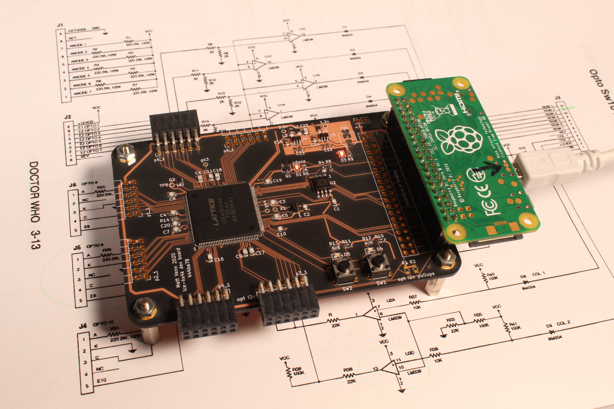
See the test program. This makes a nice pulsing effect on LED2, and LED1 is the slow PWM clock. The buttons increase or decrease pulsing speed.
make progYosys and NextPNR are used to create the bitstream and then it's copied to the Raspberry Pi specified by PI_ADDR in the Makefile.
Fomu-Flash is used to flash the SPI memory, or program the FPGA directly.
My fork of Fomu-Flash is used for programming. Fomu-Flash should be able to reconfigure the pins used with -g, but I couldn't get this to work, so I hard-coded the right pins in this fork.
| Qty | Value | Footprint | References |
|---|---|---|---|
| 17 | 100n | Capacitor_SMD:C_0805_2012Metric | C1, C2, C3, C4, C5, C6, C7, C8, C10, C11, C16, C17, C18, C19, C20, C23 +1 |
| 8 | 10k | Resistor_SMD:R_0805_2012Metric | R1, R2, R3, R4, R5, R8, R10, R11 |
| 6 | Conn_02x06_Odd_Even | Connector_PinSocket_2.54mm:PinSocket_2x06_P2.54mm_Horizontal | J3, J4, J5, J6, J7, J8 |
| 5 | 200R | Resistor_SMD:R_0805_2012Metric | R6, R9, R12, R13, R14 |
| 4 | 1u | Capacitor_SMD:C_0805_2012Metric | C12, C13, C14, C15 |
| 4 | LED | LED_SMD:LED_0805_2012Metric | D1, D3, D4, D5 |
| 4 | MountingHole_Pad | MountingHole:MountingHole_3.2mm_M3_Pad | H1, H2, H3, H4 |
| 3 | L | Inductor_SMD:L_0805_2012Metric | L1, L2, L3 |
| 2 | Conn_02x20_Odd_Even | Connector_PinSocket_2.54mm:PinSocket_2x20_P2.54mm_Vertical | J2, J9 |
| 2 | SW_Push | Button_Switch_THT:SW_PUSH_6mm | SW1, SW2 |
| 1 | 1.2v | TestPoint:TestPoint_THTPad_D1.0mm_Drill0.5mm | TP6 |
| 1 | 2.5v | TestPoint:TestPoint_THTPad_D1.0mm_Drill0.5mm | TP8 |
| 1 | 3.3v | TestPoint:TestPoint_THTPad_D1.0mm_Drill0.5mm | TP7 |
| 1 | CP | Capacitor_SMD:CP_Elec_5x5.4 | C21 |
| 1 | Conn_01x02 | Connector_PinHeader_2.54mm:PinHeader_2x01_P2.54mm_Vertical | J1 |
| 1 | D | Diode_SMD:D_0805_2012Metric | D2 |
| 1 | IS25LP016D-JBLE | Package_SO:SOIC-8_5.23x5.23mm_P1.27mm | U2 |
| 1 | Q_NMOS_GSD | Package_TO_SOT_SMD:SOT-23 | Q1 |
| 1 | SiT2001B | Package_TO_SOT_SMD:SOT-23-5 | X1 |
| 1 | TLV73312PDBV | Package_TO_SOT_SMD:SOT-23-5 | U3 |
| 1 | TLV73333PDBV | Package_TO_SOT_SMD:SOT-23-5 | U4 |
| 1 | clock | TestPoint:TestPoint_THTPad_D1.0mm_Drill0.5mm | TP5 |
| 1 | gbin3 | TestPoint:TestPoint_THTPad_D1.0mm_Drill0.5mm | TP1 |
| 1 | gbin4 | TestPoint:TestPoint_THTPad_D1.0mm_Drill0.5mm | TP2 |
| 1 | iCE40-HX4K-TQ144 | Package_QFP:TQFP-144_20x20mm_P0.5mm | U1 |


fabPlane/x68000-midi
X68000 MIDI and 8 MB RAM expansion card: Gowin GW1NR-9, YM3802-compatible gateware in Amaranth, and a universal I/O slot breakout. CC0.

mattvenn/basic-ecp5-pcb
Reference design for Lattice ECP5 FPGA. Featuring Raspberry Pi interface and 6 PMODs


gnilsson2/YAPP_Box_KiCad_Generator
Generate Openscad boxes from KiCad PCB files.

thegamer3-141/16bit_transistor_computer
A 16-bit computer built from discrete transistors, inspired by Ben Eater's famous 8-bit breadboard computer project.
It measures 100 × 68 mm and has 2 copper layers, 1.6 mm thick.
70 parts, built around the IS25LP016D-JBLE, TLV73312PDBV and TLV73333PDBV. The full list of its parts is on this page, with links to each part's symbol and footprint where PCBKit's library has them.
From the mattvenn/first-fpga-pcb repository on GitHub, at the commit this page was made from: the board is hardware/first-fpga-pcb.kicad_pcb. PCBKit opens the board in the browser, with nothing to install.
Its repository states no licence, so its author keeps all rights: ask mattvenn before reusing the design.