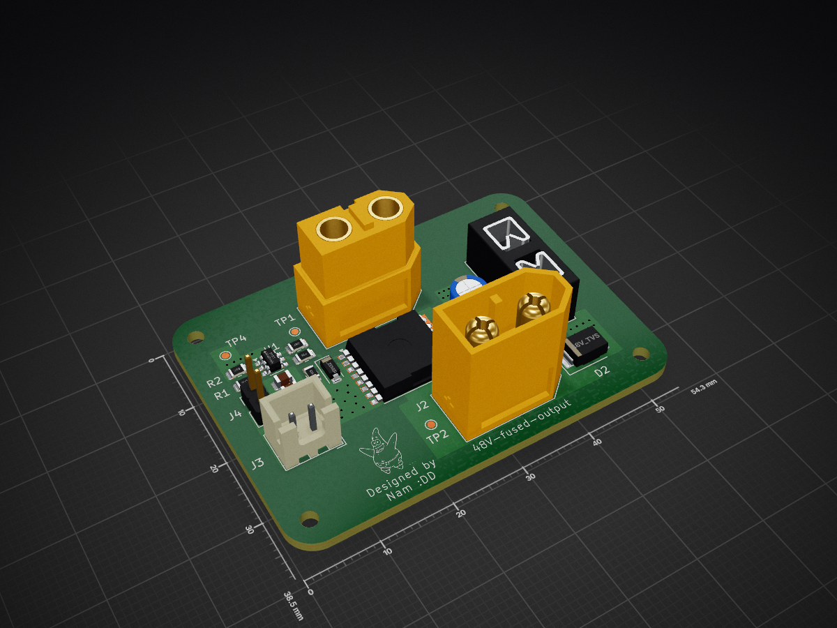
48 V Wheel Power Switch and Gate Driver
KiCad prototype design for switching the return path of a wheel module on a shared nominal 48 V bus. A 3.3 V STM32 enable signal controls an N-channel MOSFET through an Infineon 1EDN7550B gate driver powered by an assumed external regulated 12 V supply.
Status: PCB sent for fabrication (November 4, 2026). Expected arrival in approximately two weeks; assembly, bring-up and hardware validation pending.
Latest checkpoint — fabrication submitted
The editable KiCad PCB, schematic, project settings, custom libraries, and BOM are synchronized from the supplied project archive. Gerber layers, plated/non-plated drill files and the original manufacturing ZIP are included.
- Supply: confirmed 12S battery, 50.4 V maximum charged voltage.
- Design target: 10 A continuous per wheel; not yet a measured board rating.
- One wheel per board; four copper layers.
- The supplied BOM still has no manufacturer part numbers for D1, D2 or F1. Component selection and protection coordination remain open before assembly/testing.
- No independent ERC/DRC or hardware validation was performed as part of this repository update.
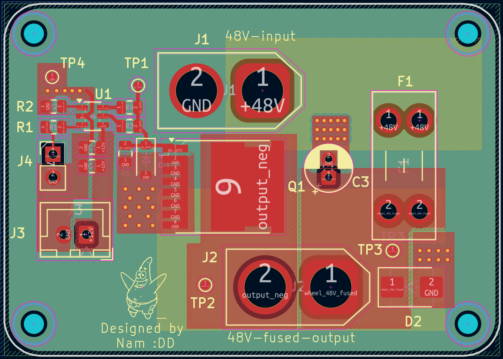
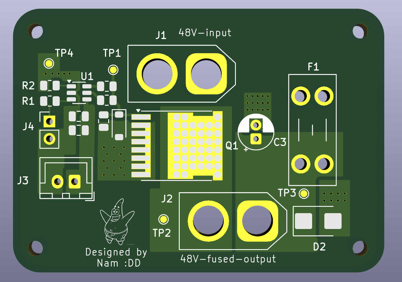
Design and manufacturing files
Earlier checkpoints below describe their status at the time; their screenshots are historical.
Previous checkpoint — third layout iteration
This checkpoint uploads the editable KiCad PCB, schematic and project settings directly from the supplied October 25 project ZIP, along with its project-local libraries and three new screenshots.
- Added C3, a 1 µF through-hole input capacitor across fused 48 V and GND.
- Added four M2 mounting holes and rounded board corners.
- Refined placement, copper zones and silkscreen.
- Proposed four-layer, 1.6 mm stackup: 2 oz outer copper and 1 oz inner copper. Actual fabrication stackup remains to be confirmed.
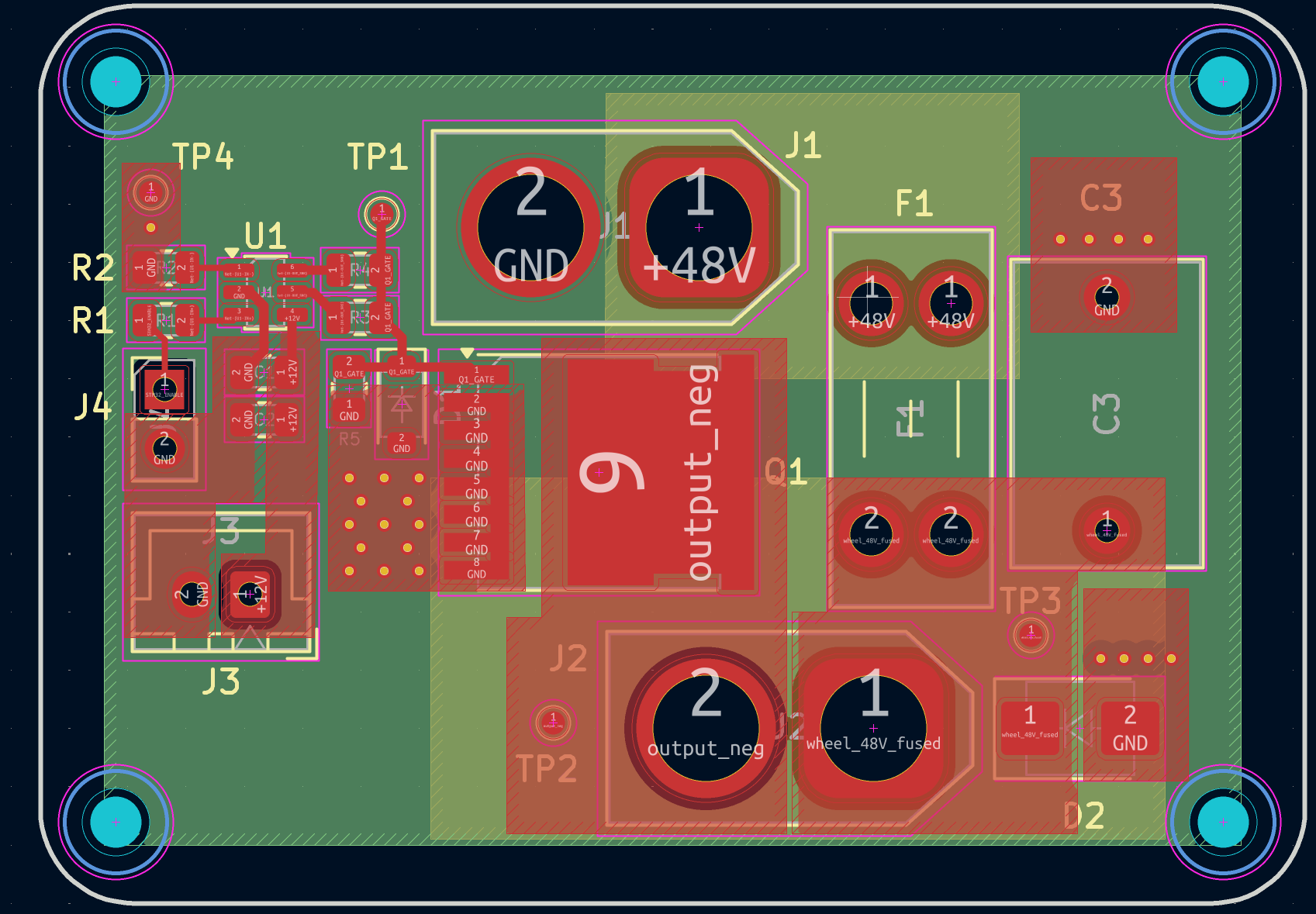
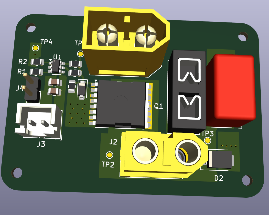
Validation status: no independent ERC/DRC, fabrication review or hardware testing was performed for this upload. Continuous-current capability is not established. The 30 A rating of the Keystone 3568 holder is a component constraint, not a verified board rating; the fuse itself and protection parts still require final selection. The native files are preserved as supplied.
Previous checkpoint — second layout iteration
The team lead approved the schematic to proceed to layout on October 1, 2026. This update saves the second placement, routing and copper-zone iteration in ProtectionGateDriver.kicad_pcb, with the supplied project settings and libraries.
The scope is one wheel per board, with six separate one-wheel boards intended for the rover. Layout review, component-rating confirmation, current-path/thermal review and hardware validation remain outstanding. This upload is a development checkpoint, not a fabrication release. ERC/DRC were not independently rerun for this upload.
Layout preview — iteration 2, not for fabrication
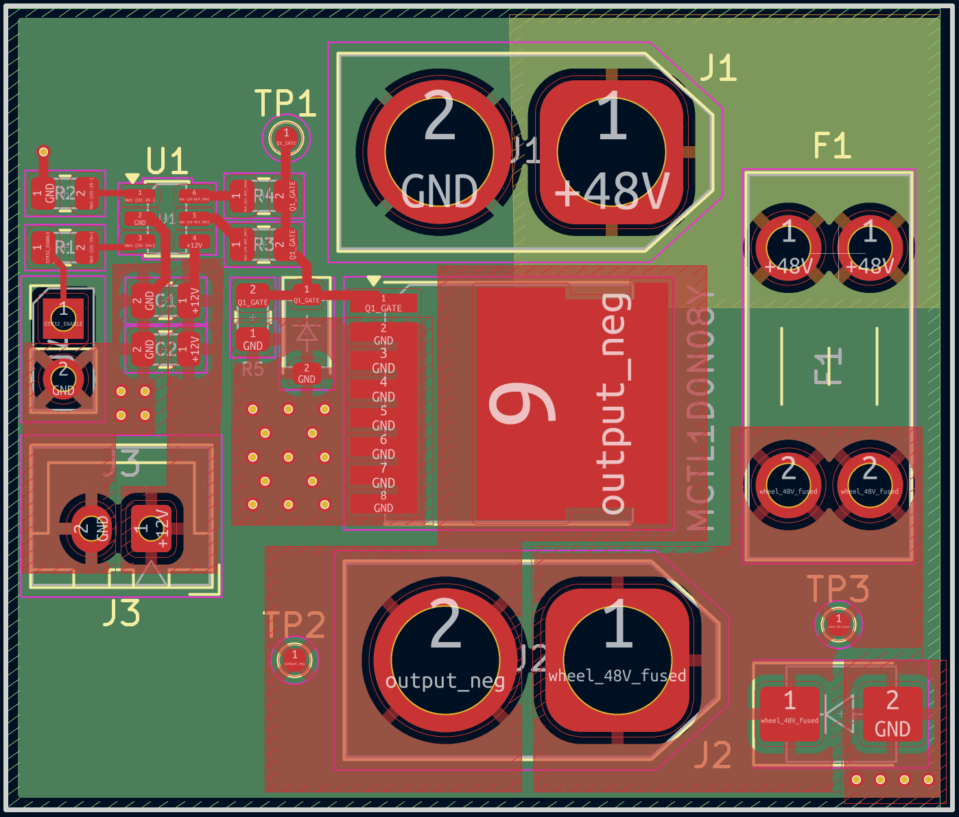
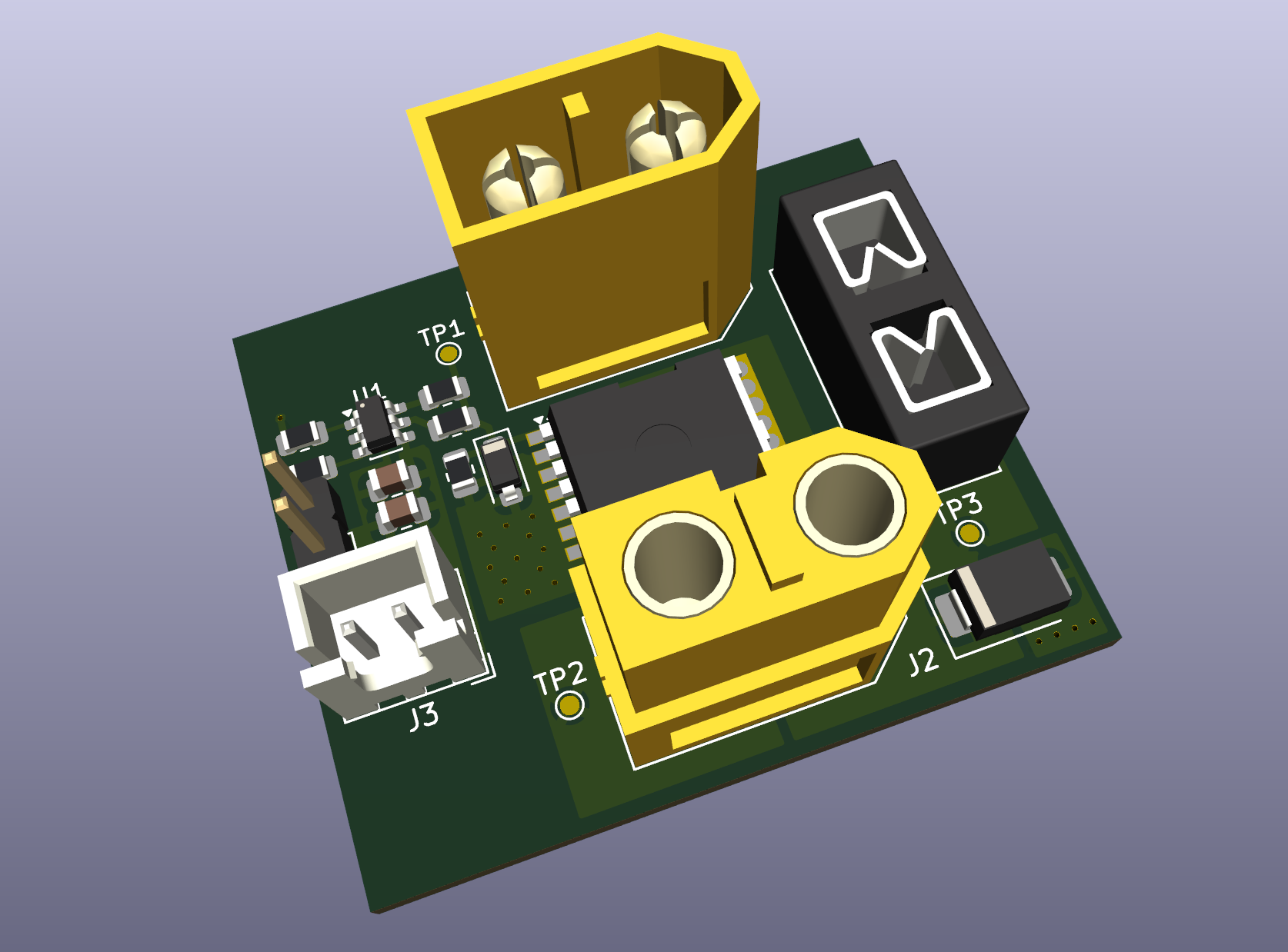
This iteration uses four copper layers (F.Cu, In1.Cu, In2.Cu and B.Cu), revised placement/routing, copper fills and ground vias. The uploaded native project files are preserved as supplied; this upload does not constitute an electrical design review.
The 3D image is a CAD preview, not a manufactured or tested board.
Previous checkpoint: iteration 1 layout and 3D preview.
Circuit overview
The description below refers to the synchronized editable KiCad files.
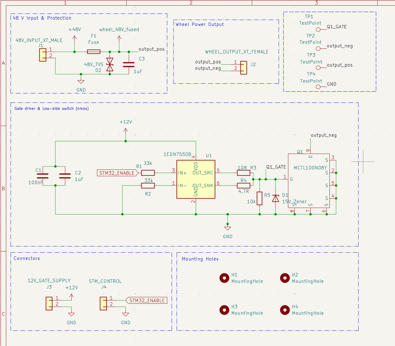
The intended load-current path is: J1 pin 1 (+48 V input) → fuse F1 → wheel_48V_fused → J2 pin 1 → external wheel load → J2 pin 2 (output_neg) → Q1 drain → Q1 source → GND → J1 pin 2.
- Q1: MCC MCTL1D0N08Y, with custom symbol and adapted TOLL-8L footprint.
- U1: 1EDN7550B, with separate turn-on and turn-off gate resistors.
- Gate-source pulldown and Zener clamp; local driver-supply decoupling.
- J1:
48V_INPUT_XT_FEMALE, with +48 V and GND input connections.
- J2:
WHEEL_OUTPUT_XT_MALE, with wheel_48V_fused and switched return output_neg.
- Driver supply: external regulated +12 V through J3; STM32 enable and GND through J4.
- D2 is connected between the fused positive supply and GND, after F1.
- Fuse and bus TVS are provisional and require selection against system requirements.
Schematic preview — work in progress
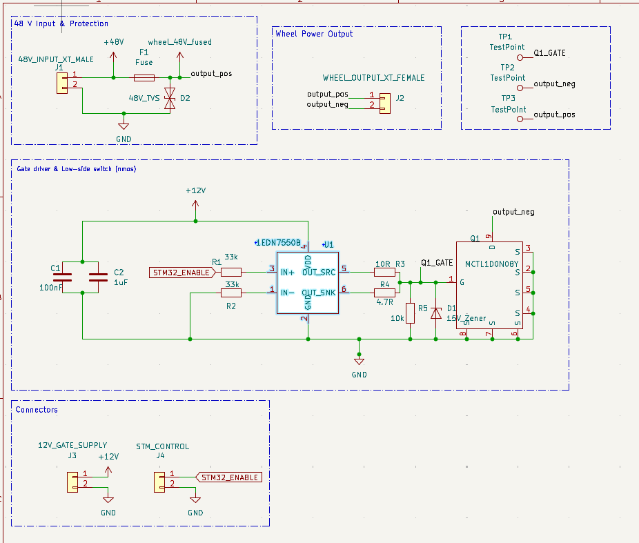
Updated preview (October 9, 2026): supplied schematic showing input protection, wheel output, gate driver, test points and external supply/control connectors. Functional blocks connect through net labels. Layout refinement and hardware validation remain outstanding.
Design calculations — preliminary
These are original working notes from the schematic, not measured results. The corrections and limitations below take precedence over statements in the screenshots.
Input and gate-drive sizing
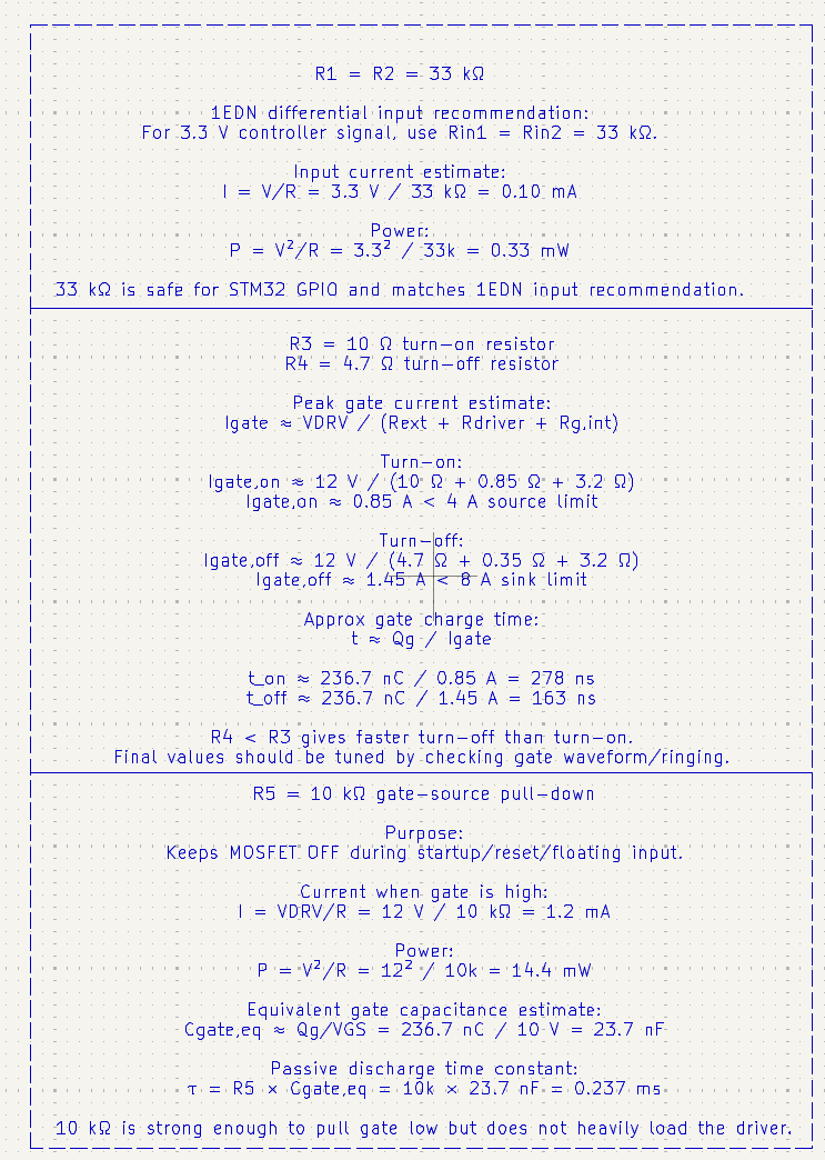
- Arithmetic check:
3.3² / 33,000 = 0.00033 W = 0.33 mW, consistent with the image. The 0.10 mA figure assumes the full 3.3 V across one resistor; actual input current and resistor dissipation depend on the driver's differential input network and common-mode voltage.
- The approximately 0.85 A turn-on and 1.45 A turn-off figures are initial resistive estimates. Gate current varies during switching;
Qg / Ipeak does not establish actual switching times. The listed 278 ns and 163 ns are rough estimates requiring waveform validation.
Qg / VGS and the resulting 0.237 ms pulldown time constant are simplified approximations for a nonlinear gate. R5 discharges an undriven gate; it does not override a driver commanded high or alone guarantee safe behavior with floating control inputs.236.7 nC / 0.25 V = 0.947 µF is a first-order charge-balance estimate. Final decoupling must account for effective capacitance at 12 V, tolerance, ESR/ESL and layout; a nominal 1 µF capacitor does not guarantee that effective value.
Gate clamp and bus protection
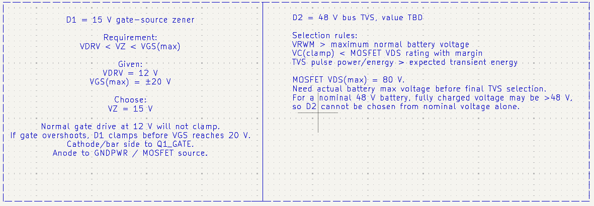
A nominal 15 V Zener does not by itself guarantee that gate voltage remains below 20 V. Verify its actual clamp voltage at the expected pulse current, tolerance and wiring inductance. TVS peak power (W) and pulse energy (J) must be checked separately against the transient waveform. Final fuse and TVS parts remain TBD.
Open the project
Use KiCad 9. Open ProtectionGateDriver.kicad_pro, then the schematic. Keep the project files, library tables, symbol library and ProtectionGateDriver.pretty folder together. Both library tables use project-relative paths.
Q1 uses ProtectionGateDriver:MCC_MCTL1D0N08Y_TOLL8L: gate pad 1, source pads 2–8, drain pad 9. Source pads share connected copper. The footprint was adapted from KiCad's Package_TO_SOT_SMD:Infineon_PG-HSOF-8-1; inherited geometry and 3D model still need dimensional review. Upstream KiCad library licensing applies to derived library content; see https://www.kicad.org/libraries/license/.
Repository baseline and completed milestones
- Received team-lead approval for the latest local schematic to proceed to PCB layout (status recorded October 1, 2026).
- Captured the low-side switching circuit and STM32 enable interface in the repository baseline.
- Synchronized the approved local schematic and project files; J1 is the 48 V input and J2 is the wheel output.
- Added a project-local MOSFET footprint with pad numbering matching the custom symbol.
- Checked edited schematic structure and connector wire paths programmatically. These checks do not replace KiCad ERC or hardware tests.
Next steps — assembly and validation
- Receive and inspect the fabricated PCBs; check dimensions, footprints and continuity.
- Complete the BOM and review fuse, gate Zener and bus TVS choices against the 50.4 V battery and expected transients.
- Confirm the motor/controller interface, startup/stall current and grounding architecture.
- Assemble and bring up the board with a current-limited supply.
- Measure gate/drain waveforms, voltage drop and temperature rise before claiming 10 A continuous capability.
- Record test conditions, results and any changes needed for the next revision.
No hardware performance is claimed. An RC snubber is not present in this revision.
References