Skip to the content
PCBKitNew board
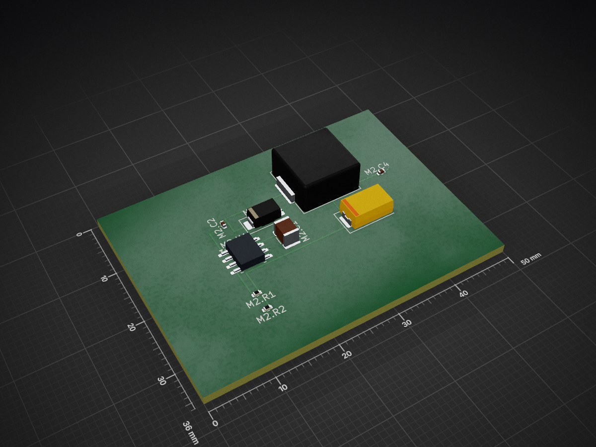
2 layers50 × 36 mmCharger buck, the printed circuit board in 3D

Charger buck

luffffyz/TextEDA

Agent first, human reviewable. Describe schematics and PCBs as text: typed IR, validators, KiCad export, and a reference renderer.

Size
50 × 36 mm
Copper layers
2
Thickness
1.6 mm
Parts
9
Nets
6
Pads
30
Tracks, vias
29, 7
Pours
1
Routed
Yes
KiCad
KiCad 0.1 (file 20241229)
Created
20 Oct 2026
Updated
5 Nov 2026

Overview

Charger buck is an open-source printed circuit board by luffffyz, from the luffffyz/TextEDA repository on GitHub, published under the Apache-2.0 licence. It is a 2-layer board of 50 × 36 mm with 9 parts on 6 nets, routed with 29 tracks and 7 vias.

It is built around the TPS5430DDAR, B340A and IHLP4040DZER150M11. It belongs with the power boards of this library.

Main components

3

README

docs/trial-run/charger-buck/README.md

试跑记录:pcb 描述 → KiCad → DRC / Gerber

日期:2026-10-20 · 门:docs/adr/0005-manufacturing-output.md decision 8(试跑门)· KiCad 10.0.7

历史快照:本目录记录的是自建库落地之前的一次试跑,板里的封装来自 KiCad 官方库(见本目录 fp-lib-table 里的 nix 路径)。参考工程自此全部自建(docs/adr/0013-reference-project-self-built-libraries.md),当前的库级闭环门槛是 bun run lib:verify;本目录的产物保留作为当时的证据,不代表现在的库。

试的是什么

examples/reference-project 的 charger-buck 板。输入是仓库里的 pcb 描述 examples/reference-project/design/pcb/charger-buck.teda(层:pcb / B0), 输出是本目录下的 KiCad 板文件、工程文件、DRC 报告与 Gerber 清单。

这块板不是量产板:sch 展平后有 M1(charger-power,60 个器件)与 M2(buck-5v,9 个器件)两个页面, 本描述只放置了 M2 页的 9 个器件,M1 页按 spec/pcb.md §5.2 规则 1 视为变体状态(不贴)。 它验证的是链路(描述 → KiCad → DRC → 制造文件),不是这块板的设计。

怎么跑

sh
kicad-cli pcb drc --format json --severity-all --refill-zones -o drc.json charger-buck.kicad_pcb
kicad-cli pcb export gerbers --check-zones --output gerbers/ charger-buck.kicad_pcb
kicad-cli pcb export drill  --output drill/  charger-buck.kicad_pcb

--check-zones 必须带:.kicad_pcb 里只写铺铜多边形,填充结果不在文件里;不带这个开关导出的 B_Cu 只有过孔、没有铜皮(实测:703 B → 1158 B,缺 G36/G37 填充区)。

板文件由一次性原型(未进仓库)从 examples/reference-project/design/pcb/charger-buck.teda 生成,导出器本体是 P2 的活。 本目录里的 charger-buck.kicad_pcb 与仓库里的输入逐字节一致(原型是确定性的:uuid 由内容派生)。

charger-buck.kicad_pro 必须与板文件同目录——设计规则在工程文件里,不在 .kicad_pcb 里(见 docs/kicad-pcb-format.md)。 fp-lib-table 同理:没有它,KiCad 会对每个封装报 lib_footprint_issues(9~10 条 warning),DRC 报告就不干净。

结果

项结果
DRC 违规0(drc.json:violations: [])
未连接项0(unconnected_items: [])——connect 段与几何一致,展平网表被完整走通
Gerber21 个文件(双层铜、阻焊、锡膏、丝印、装配/用户/eco 层、板框、courtyard、fab、*.gbrjob)
钻孔1 个 Excellon 文件(charger-buck.drl)

板上有 6 个 net:板级 GND / SYS / VOUT,页内 M2.BOOT / M2.PH / M2.VFB(命名规则见 docs/adr/0007-page-internal-net-naming.md)。

这轮试跑查出来的东西

  1. IR 的 rules 段没有 .kicad_pcb 落点——板文件里根本不含设计规则,DRC 跑的是 KiCad 默认值。 规则必须写进 .kicad_pro(design_settings.rules + net_settings.classes)。 已实测:把 min_clearance 改成 1.0mm 后 DRC 立刻报 40 条 clearance 违规 → 工程文件确实生效。
  2. 页内 net 的命名缺口(docs/adr/0007-page-internal-net-naming.md):teda.md §7.7 原来写"页内 net 不参与板级 net", 而 pcb 又必须连它,两条规则放在一起无解;且两个页面各有同名 PH/VFB。已定命名规则并改了 teda.md §7.7、spec/pcb.md §5.1/§5.2。
  3. 封装 pad 的角度是绝对角:板文件里 pad 的 at 角度 = 库里的角度 + 实例旋转(已与 KiCad 官方模板板比对确认), 而 pad 的坐标仍是封装局部坐标(未旋转)——位置与角度的旋转规则不一样,容易写错。
  4. 库绑定要有落点:封装在板文件里是内联的((footprint "LIB:NAME" ...)),但 LIB:NAME 仍被 KiCad 当库引用去核对, 没有 fp-lib-table 就报 lib_footprint_issues。
  5. 铺铜填充不在板文件里:zone 只写多边形,填充由 KiCad 算且不写回文件;pcb export gerbers 必须带 --check-zones, 否则导出的背面铜只有过孔、没有铜皮。DRC 那边对应的是 --refill-zones。

没验到的(下一轮)

  • 叠层没落进去:stackup 段(铜厚、介质厚度、材料)在本轮只落了 board_thickness → (general (thickness 1.6)); 完整叠层应写进 .kicad_pro 的 design_settings.stackup,本轮没做。
  • mask / paste / thermal / min_width 四个 rules 参数没验:它们按 ADR 0005 decision 5 是封装属性与zone 属性,不是板级设置,落点要单独核。
  • 板框:本轮用 4 条 gr_line 拼矩形;多边形板框、gr_rect、圆角都没试。
  • 槽孔、非镀通孔、双面器件、背面丝印都没试(physical_only 段还没实现)。
  • Gerber 只验了文件齐全与可导出,没有做 CAM 级检查(阻焊扩张、锡膏比例、孔环)。
  • 布线是一次性原型算的,不是布局布线器;真实项目要接 freerouting / KiCad。

Parts

9
QtyValueFootprintReferences
2c-0402Capacitor_SMD:C_0402_1005MetricM2.C2, M2.C4
2r-0402Resistor_SMD:R_0402_1005MetricM2.R1, M2.R2
1B340ADiode_SMD:D_SMAM2.D1
1IHLP4040DZER150M11Inductor_SMD:L_Vishay_IHLP-4040M2.L1
1TPS5430DDARPackage_SO:SOIC-8-1EP_3.9x4.9mm_P1.27mm_EP2.95x4.9mm_Mask2.71x3.4mmM2.U1
1c-1210Capacitor_SMD:C_1210_3225MetricM2.C1
1c-220uCapacitor_Tantalum_SMD:CP_EIA-7343-20_Kemet-VM2.C3

Questions

How big is the Charger buck PCB?

It measures 50 × 36 mm and has 2 copper layers, 1.6 mm thick.

What parts does the Charger buck use?

9 parts, built around the TPS5430DDAR, B340A and IHLP4040DZER150M11. The full list of its parts is on this page, with links to each part's symbol and footprint where PCBKit's library has them.

Where can I download the Charger buck KiCad files?

From the luffffyz/TextEDA repository on GitHub, at the commit this page was made from: the board is docs/trial-run/charger-buck/charger-buck.kicad_pcb. PCBKit opens the board in the browser, with nothing to install.

Can I use the Charger buck design in my own project?

Its repository publishes it under the Apache-2.0 licence: you may reuse it on that licence's terms (keep the author's notice, and for a copyleft licence share your changes alike).

Similar boards

  • 2 layers59 × 88.5 mmKHNATH002 Power System, the printed circuit board in 3D

    KHNATH002 Power System

    Athenkosi-Khonzani/MEERKAT_Underwater_Ice_Detection_And_Avoidance-System

    MEERKAT is a small, low-cost Autonomous Underwater Vehicle (AUV) designed to detect and avoid sub-surface ice (frazil ice, brash ice, and submerged keels of icebergs) in turbid polar waters.
    45 parts
  • 6 layers152.4 × 94 mmESP32-Sequencer v0.2, the printed circuit board in 3D

    ESP32-Sequencer v0.2

    brokebit/PA-Sequencer-Hardware

    Sequencer for a Power Amplifier

    125 parts
  • 6 layers110.9 × 93 mmESP32-Rotator v0.2, the printed circuit board in 3D

    ESP32-Rotator v0.2

    brokebit/Rotator-ESP32-S3-Board

    Rotator Controller based on an ESP32-S3 micro and Clearpath Servos

    89 parts
  • 6 layers90 × 90 mmSolarDataLogger, the printed circuit board in 3D

    SolarDataLogger

    brokebit/SolarDataLogger

    Firmware for custom data logger for Victron MPPT charge controllers via the Ve.Direct port/protocol.

    70 partsCC0-1.0
  • 4 layers100 × 64.9 mmSensorBoard, the printed circuit board in 3D

    SensorBoard

    VogelPapaFinn/SensorBoard_PCB

    127 parts
  • 4 layers69.9 × 38.9 mmLoRA board, the printed circuit board in 3D

    LoRA board

    SCFormulaElectric/USC-Electrical-Systems

    67 parts9
  • 4 layers80 × 104.1 mmRobuoy Sub, the printed circuit board in 3D

    Robuoy Sub

    pnn69/Kicad_PCB

    Schematics and PCB's designed with Kicad

    141 parts
  • 4 layers100 × 68 mmDevKit, the printed circuit board in 3D

    DevKit

    kaminaris/GigaESC

    209 parts47