2 layers88.6 × 30 mm

 lrrosa/tia-fpga1
FPGA replacement for the Atari 2600 TIA (C010444) video/sound chip, targeting a Sipeed Tang Nano 9K. Open hardware, CERN-OHL-S-2.0.
Tia fpga is an open-source printed circuit board by lrrosa, from the lrrosa/tia-fpga repository on GitHub, published under the CERN-OHL-S-2.0 licence. It is a 2-layer board of 61.6 × 34.5 mm with 24 parts on 93 nets, routed with 640 tracks and 48 vias.
It is built around the 74LVC2G07GV and MBR0540. Its parts include 10 capacitors, 9 ICs, 4 connectors and 1 diode. It belongs with the fPGA and programmable logic and audio and music boards and the FPGA and CPLD boards of this library.


An FPGA replacement for the Television Interface Adaptor (TIA) — the custom
C010444 / C010444D (NTSC) video and sound chip of the Atari 2600.
Revision B is the digital interface board between a Sipeed Tang Nano 9K module and the TIA's DIP-40 socket, for use with a real 6507 (on a breadboard or in an actual 2600). Revision A, the first study, was never built.
| Front | Back |
|---|---|
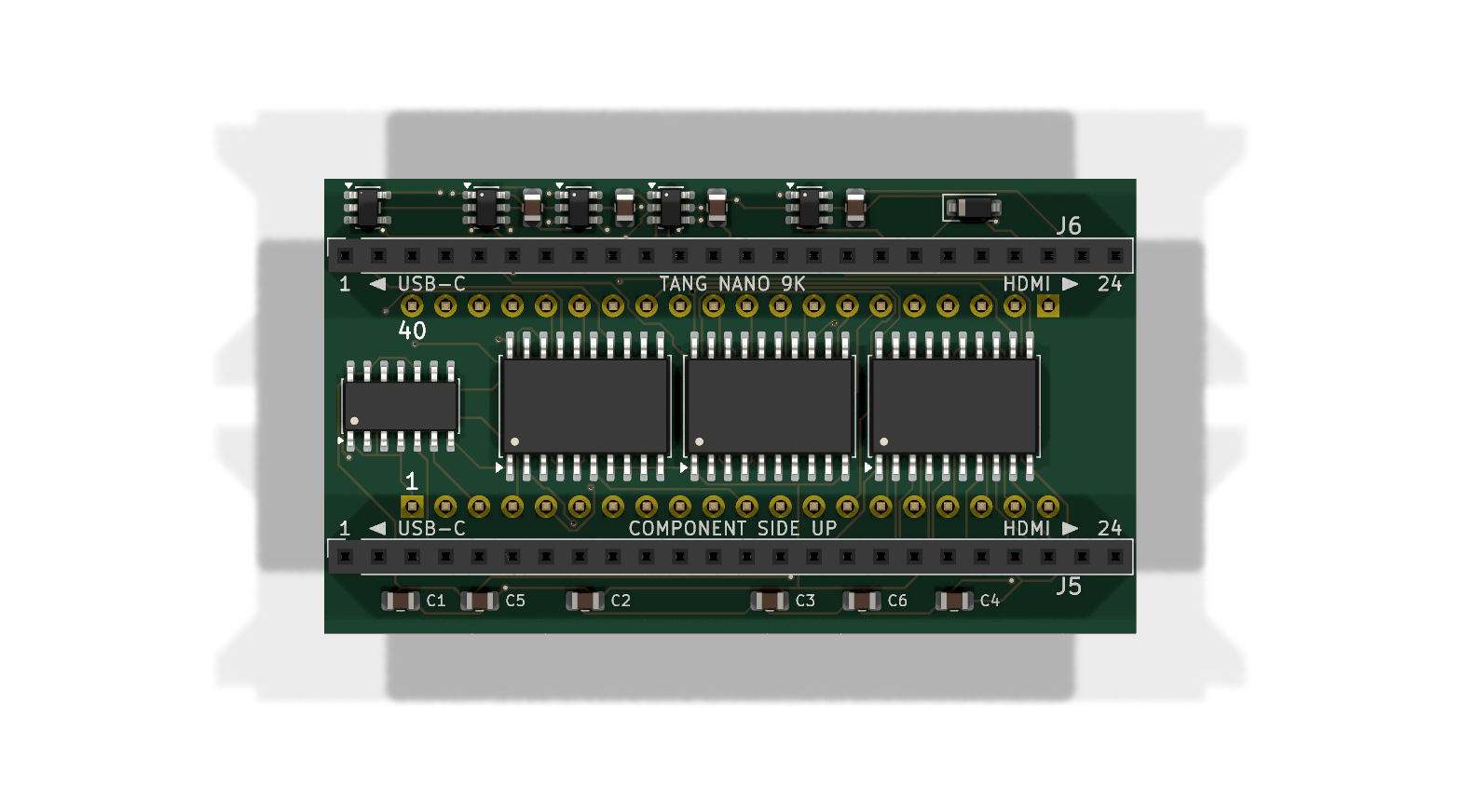 | 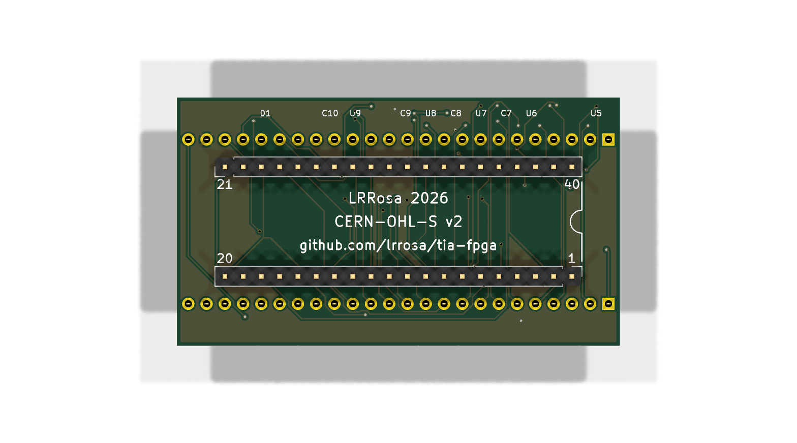 |
| Tang Nano sockets face up; the logic sits in the channel between the rows | The TIA's DIP-40 pins face down into the socket, over the ground pour |
61.6 × 34.54 mm, two layers. Every row lands on the 2.54 mm grid — the DIP-40's 15.24 mm and the Tang Nano's 22.86 mm — and the board is a little shorter than the module it carries, as it has to be: in a real 2600 the TIA, the 6507 and the RIOT sit millimetres apart.
The TIA has 6,193 transistors — 1,657 of which are NMOS pull-ups, leaving about 4,500 of actual logic. It fits in any modern FPGA with room to spare: synthesising a known implementation yields 311 flip-flops and roughly 2,200 basic gates.
Size was never the problem. Two other things are:
DEL). It has no direct
digital equivalent.This revision solves (2) and leaves (1) for later.
| Ref | Part | Function |
|---|---|---|
| J1, J4 | 1x24 sockets | Sipeed Tang Nano 9K module (GW1NR-LV9QN88PC6/I5): J1 takes its J6 row, J4 its J5 |
| J2, J3 | 1x20 SIP strips | Plug into the DIP-40 socket in place of the C010444 |
| D1 | MBR0540 | Feeds the module's 5 V pin from the socket, and blocks its USB from feeding the console |
| U1 | 74AHCT125 | Φ0 and RDY buffer, powered from +5 V. The critical part |
| U2 | 74LVC245A | D0–D7 bidirectional bus. A side = FPGA, B side = TIA |
| U3 | 74LVC541A | A0–A5 and R/W into the FPGA; Φ2 buffered to a spare pad |
| U4 | 74LVC541A | /CS0, /CS3, triggers I4/I5 and the 3.579545 MHz crystal clock |
| U5 | 74LVC1G32 | /CS0 OR /CS3: /OE for the 245, and the FPGA's chip select |
| U6–U9 | 74LVC2G07 | Open-drain drivers for SYNC, LUM0–2, COL, BLK, AUD0 and AUD1 |
The video and sound pads — SYNC, LUM0–2, COL, BLK, AUD0 and AUD1 — each go through one channel of U6–U9. On the die every one of them is a pull-down transistor and nothing more; the buffers make the board's pins the same, open drain and 5 V tolerant, so the console's own pull-ups set every level. See Pads and levels below.
Pin 10 (DEL) is marked no-connect: it is the colour trim pot, which has no
function in a replacement.
Neither of the 245's control lines comes from the FPGA. The A side faces the
FPGA, so DIR can be driven straight from the buffered R/W (DIR=1, a read,
sends FPGA → TIA), and /OE comes from U5. That is deliberate — see the pin
budget below.
The Tang Nano 9K's headers are 2×24, but only 29 of those 48 pins are usable 3.3 V GPIO:
| Count | ||
|---|---|---|
| J5 pins 1–22 | 22 | banks 1/2 at 3.3 V — all usable |
| J6 pins 1, 10, 11, 19–22 | 7 | 3.3 V — usable |
| J6 pins 2–9 | 8 | BANK3 at 1.8 V — not usable at 3.3 V |
| J5 23–24, J6 12–17 | 8 | HDMI differential pairs — not GPIO |
| J6 18, 23, 24 | 3 | +5V (fed through D1), GND, +3V3 |
Verified against both revisions of the official Sipeed board schematic (3672 and 3674), which agree exactly. Many of the 29 are shared with onboard peripherals (SD card, RGB LCD, SPI LCD); they are free to reuse as long as you do not fit those.
Rev B uses all 29 with nothing spare. A fully featured TIA needs about 36.
BLK has its pin because the FPGA reads /CS0 OR /CS3 from U5, which makes it
for the 245 anyway, instead of taking the two selects separately.
Chroma is fitted. F_COL took the pin that used to carry Φ2, and that trade
is deliberate rather than grudging: the FPGA generates Φ0 itself, so it knows
where it is in the bus cycle and can time accesses off its own clock instead of
the 6507's output. It costs a little timing fidelity and buys back colour on the
composite and RF path — which is the difference between a board that only works
with an HDMI monitor and one that revives a console with a dead TIA while
keeping its original video. Φ2 is still buffered by U3, brought out to an
unconnected pad for a future revision.
What still does not fit: the four paddle inputs plus their dump/compare control.
Two ways to get the remaining pins back:
docs/bare-fpga.md.This is the single most important thing to know before ordering parts: the Tang Nano 9K is big enough in logic by a wide margin, and tight in pins. Every compromise in this design traces back to that.
Rev B is a 2-layer, 61.6 × 34.54 mm board — shorter than the Tang Nano it carries. In a real 2600 the TIA, the 6507 and the RIOT sit millimetres apart, ringed by resistor networks and the cartridge slot, so the board cannot spread sideways. The two sets of rows face opposite ways:
| y (mm) | Row | Side | Faces |
|---|---|---|---|
| 5.84 | J1 — Tang Nano J6 | F.Cu | socket, up |
| 9.65 | J3 — TIA pins 21–40 | B.Cu | pins, down into the socket |
| 24.89 | J2 — TIA pins 1–20 | B.Cu | pins, down |
| 28.70 | J4 — Tang Nano J5 | F.Cu | socket, up |
Both pitches land on the 2.54 mm grid: the DIP-40 rows 15.24 mm apart, the Tang Nano's 22.86 mm, and the DIP pair centred between the sockets — 3.81 mm of gap on each side. Which socket takes which module row is not free — see Which row is which. SMD logic sits on the front in the 15.24 mm channel between the DIP rows. The open-drain drivers and their capacitors sit in the top margin, right above the TIA pins they drive, with D1 beside them, and the channel's decoupling in the bottom margin.
| Size | 61.6 × 34.54 mm, 2 layers |
| Components | 24 — SOIC/SOT-23 logic, 0805 capacitors, one diode, through-hole connectors |
| Routing | 640 segments, 48 vias, 1.84 m of copper |
| Ground | B.Cu pour, 721 mm² in four islands, tied together by track |
| Track / clearance | 0.18 mm / 0.13 mm |
| DRC | 0 violations, 0 unconnected pads |
Which signal sits on which header position is free — any GPIO can carry any
signal — so it is chosen to put each FPGA pin as close as it can be to the pad
its net really reaches: the buffer or gate between it and the TIA socket, not
the socket pin beyond it. Solved as an assignment problem (Hungarian, over the
29 usable positions, Manhattan distance to those pads), the whole set comes to
571 mm. F_OSC is held to J6/1, the right PLL's own input, which costs 25.6 mm
of that and keeps the colour clock off the FPGA's general routing.
The sum is what the module's own geometry allows: J5 carries 22 of the 29 signals, and the buffer or gate each one reaches sits in the channel between the two TIA rows, so most of the bus crosses that channel whatever the assignment does. Solving it still beats the alternative — the same signals laid out by hand come to 685 mm.
Rev A measured the distance to the TIA pin itself, which left out the detour through the buffers: its data and chip-select lines crossed the board twice. The buffers stay ordered left to right by the centroid of what they carry, U1, U4, U3, U2, and against rev A the board saves copper while gaining five parts:
| rev A | rev B | |
|---|---|---|
| Segments | 601 | 534 |
| Vias | 31 | 39 |
| Copper | 1.68 m | 1.48 m |
fpga/tia_fpga.cst carries the result. Do not reshuffle those IO_LOC lines
casually — the layout depends on them.
Autorouted with Freerouting 2.2.4: all 120 nets in about 12 s but three ground connections. Two are closed with a via dropped on the branch's own track where it passes over the pour, and the last two capacitors are tied to their neighbours along the free lane that runs just inside the top edge. The channel leaves only ~1.1 mm between the header pads and the SOIC pads, so the geometry decides whether it routes at all: it takes 0.13 mm clearance and 0.18 mm track. The ground pour is added after routing — Freerouting reads a pour as an obstacle and goes effectively single-layer if one is present.
Files: tia-fpga.kicad_pcb, renders in docs/, fabrication output in gerbers/.
The files in gerbers/ are ready for any PCB house as they are — Gerber X2
plus Excellon drill, with FABRICATION-NOTES.txt alongside them; zip them with
the files at the root of the archive. Nothing in it needs more than standard
low-cost capability:
| Size / layers | 61.6 × 34.54 mm, 2 layers, 1.6 mm FR4 |
| Min track / clearance | 0.18 mm / 0.13 mm |
| Drills | 0.30 mm (vias), 1.00 mm (connectors) |
docs/bom-production.csv is the parts list with suggested orderable numbers.
Three assembly points that are easy to get wrong:
1 ◀ USB-C … TANG NANO 9K … HDMI ▶ 24 under J1 and
1 ◀ USB-C … COMPONENT SIDE UP … HDMI ▶ 24 over J4, with J6 and J5 out
in the margins beyond each socket. See
Which row is which.CERN-OHL-S v2,
LRRosa 2026 and github.com/lrrosa/tia-fpga, between the two rows of TIA
pins. The licence asks for it to travel with the board; keep it on a respin.The Tang Nano's two rows are 22.86 mm apart (9 × 2.54), from Sipeed's own
dimension drawing, Tang_Nano_9K_3672_size. Pin 1 of both rows is at the USB-C
end, 2.55 mm from that edge; the HDMI connector is at the other end and
overhangs this board by about 7.5 mm, with a millimetre of module sticking out
at the USB end as well. Both hang in free air, 20 mm above the console.
The front silkscreen carries all of this. Each socket has a strip along its
inner edge, and both read the same way: 1 ◀ USB-C at the left end, HDMI ▶ 24
at the right, and one line in the middle — TANG NANO 9K above the TIA pins,
COMPONENT SIDE UP below them. The row names, J6 and J5, sit out in the
margins past each socket instead, where the middle of the board is already
busy. The 1 and 24 are the module header's own pin numbers, not the TIA's —
the TIA's 1 and 40 sit on the other side of each pad row. Three independent
facts are printed there, and the module can only go in one way that satisfies
all three.
Looking down at the module with the USB-C end on the left, J6 is the upper
row and J5 the lower one, so J1 takes J6 and J4 takes J5. Three things say so
and agree: the pin numbers silkscreened on the module's underside, the QN88's
own pin order on the top-side photo in Sipeed's datasheet, and third-party
carrier boards for the module. On your own board, look for 63 beside pin 1
of one row and 38 beside pin 1 of the other: 63 is J6/1, which this board
wires to F_OSC.
Rev A and the first cut of rev B had both of these wrong — 20.32 mm, and the rows the other way round. Nothing was ever fabricated from them.
Until 2026-09-20 the board carried TIA pins 1–20 on the upper row with the
half moon on the left. That is impossible for a real DIP: seen from the top with
the key at the left, pin 1 is at the bottom left — KiCad's own
Package_DIP/DIP-40_W15.24mm puts pin 1 at (0,0), 1→20 running +y, 21 at
(15.24, 48.26) and 40 at (15.24, 0). Taking u = pin1→pin20 and v = pin1→pin40,
the cross product is negative for a real DIP and was positive here: a mirror,
which no rotation undoes. The board would not have worked in a console.
The silkscreen numbers were never the bug — they described the copper faithfully. The fix swapped the two rows (J2 to y 24.89, J3 to y 9.65), which keeps every signal's x and so leaves the pin assignment above untouched, and the board was re-routed from scratch. The check that misses this is "pin 21 is opposite pin 20" — true in both the correct board and the mirrored one.
The DIP-40 row spacing (15.24 mm) is fixed by the package and is not a guess.
The board needs tall pins. It overhangs the neighbouring 6507 and RIOT, which sit proud of the 2600's PCB in their own sockets. Standard DIP header pins would put this board straight into them; a socket extender or long machined pins are required. Measure the vertical clearance in your console — the Tang Nano's HDMI connector adds roughly 5 mm on top.
There are no mounting holes. The board is held by its own pins in the TIA socket, and there is nothing to screw into inside a 2600. Adding holes only forced the board larger, so they were dropped.
Reading the die's netlist for the RTL settled something the schematic had assumed. Every video and sound pad on the TIA — SYNC, LUM0–2, COL, AUD0, AUD1, and BLK and RDY too — is a pull-down transistor and nothing else. None of them can drive high. Φ0 is the only output with a real driver on both sides.
The console schematics show the other half:
| 2600A, rev 16 | 2600 (the original board) | |
|---|---|---|
| LUM0–2, SYNC | R218–R221, 3.3–4.7 kΩ to +5 V, straight into the summing resistors (R214–R217: 27, 47, 110, 24 kΩ) | R218–R221, 3.3 kΩ to +5 V, into a CD4050 run from a divider off +5 V (R231, R232: about 3.6 V), then the summing resistors (R222–R224, R234: 12, 24, 47, 10 kΩ) |
| COL | R228, 1 kΩ to +5 V; C210, 47 pF, to a second 1 kΩ pull-up (R211); 6.8 kΩ and 22 pF into the sum | R212, 1 kΩ to +5 V; C212, 47 pF, to a second 1 kΩ pull-up (R214); 22 pF and 6.8 kΩ into the sum |
| BLK | R234, 820 Ω, into the COL node (revs 14 and 15: not connected) | R213, 680 Ω, into the COL node |
| AUD0, AUD1 | joined; R206, 1 kΩ to +5 V; 0.1 µF and 18 kΩ into the sound oscillator | joined; R208, 1 kΩ to +5 V; the same coupling |
PAL consoles use a different TIA (C011903): one sound pad, AUD on pin 13 with its own 1 kΩ pull-up, while pins 12 and 8 carry the PAL signals. This board is for the NTSC chip.
Rev B follows the die:
tia_board.v still puts
the same pulse-width mix of both channels on both pins; for a console
modified for stereo, AUDIO_STEREO = 1 gives each pin its own channel, in
non-overlapping halves of the pulse frame so the two still add correctly
wherever they meet.Reviving a dead console. Pull the failed TIA, drop this in its socket, and keep the 2600's own RF modulator or composite mod. Chroma, luma, sync and audio come out on the same socket pins the original chip used, open drain as the chip's are, so the console's video path is untouched.
As a development target. Plug it into a breadboard next to a real 6507. The Tang Nano's HDMI connector would cost no header pins — its pins are dedicated differential pairs on the module — but the RTL has no TMDS encoder yet, so for now the picture comes from the socket pins, through a network like the console's.
rtl/ holds the core: horizontal counter, playfield, two players, two
missiles, ball, collisions, HMOVE, audio and the bus interface, in eleven files
of plain Verilog-2005, plus tia_board.v, which puts it on this board. sim/
holds the test harness the section below argues for, and it is not
aspirational: the core is checked against
Sim2600 half clock by half clock, on a
real game and on test cartridges written to hit each feature from every phase
that matters.
python sim/run.pyAgainst Donkey Kong from power-on to its first picture, and against every test
cartridge -- playfield, players, missiles, ball, collisions, HMOVE with Cosmic
Ark, resets at every phase of HBLANK, vertical delay and both sound cartridges
-- the core matches the die on every pin at every half clock.
sim/README.md has the table. (The Donkey Kong traces are regenerated locally rather
than committed, since they carry the game's artwork.)
Sim2600 wires one clock wrong, and both wirings are now in the suite.
Upstream Sim2600 feeds the TIA's Φ2 input from the 6507's Φ1 output, the
inverse of what the console does. The die only looks at that pin through
write strobes, so everything still worked, but every write landed on the other
half of the colour clock from where a real console puts it. With the console's
wiring (sim/patches/sim2600-phi2.patch, traces in sim/traces/phi2/), five
of the core's timing rules turned out to have been fitted to the wrong side
and were re-read from the netlist — RSYNC's restart, RDY's release, how
long a reset holds an object's clock, the size gate of stretched players and
when HMOVE's comparators see a new value. The last mismatch was a mechanism
no rule had covered: HMOVE pulses in the visible line merge into the object
clocks and show on the pads half a colour clock early. The core now matches
both sets on every pin of every trace.
The board. rtl/tia_board.v is everything between the core and the board's
pins: the core's clock from a PLL locked to the console's crystal, Φ2 rebuilt
from the Φ0 the board makes itself, the data bus, chroma as that clock shifted
in phase by hue, and sound as pulse width. fpga/tia_fpga_top.v adds the Gowin
PLL, bus buffers and chroma ODDR. sim/tb_board.v replays the console-wired
traces into the board logic and checks every pin it drives, and
fpga/build_gowin.tcl builds the bitstream with Gowin EDA — from a directory
whose path has no spaces, since Gowin's place and route will not run in one
that does.
Getting there turned up a good deal the published documentation does not say, all of it now in the source: which edge of the colour clock each latch runs on; that Φ0 is a 50 per cent square wave reloaded by the horizontal counter; what RSYNC actually does, which Towers left as "requires more investigation"; that HMOVE's first compare must come before its first decrement, or an HMxx of -8 moves an object sixteen pixels the wrong way; that HMOVE's pulses past HBLANK merge into the object clocks instead of counting; and exactly when a mid-line playfield write reaches the screen. Once the harness could record the die's internal wires as well as its pins, the netlist itself settled the rest: how a RESxx strobe really resets an object -- by holding its clock, not by zeroing its counter -- and how the sound counters are clocked, down to the discovery that the two audio channels are not wired alike.
Clocking. The real chip is clocked by the 3.58 MHz colour clock and uses
both its edges. This core takes a faster system clock and treats the colour
clock as a signal to oversample, so everything is one clock domain, one edge,
no gated clocks. On this board clk0 comes from the console's own crystal
through U4 and the system clock from a PLL, so the core stays locked to the
machine it is plugged into.
fpga/tia_fpga.cst)BLK on pin 6 — U6–U9, with
sim/tb_board.v checking BLK against the diertl/tia_board.v and fpga/tia_fpga_top.v: PLL off the
console's crystal, Φ2 rebuilt from Φ0, data bus tri-state, chroma through
an ODDR, sound as pulse width. Checked pin by pin against the traces by
sim/tb_board.vsim/patches/sim2600-phi2.patch fixes that and
sim/traces/phi2/ holds the re-recorded setsynth_gowin with no warnings — the core is
516 flip-flops and 722 LUTs, the whole board top 624 and 698, under
10 per cent of the GW1NR-9 (fpga/check_synth.py)fpga/build_gowin.tcl). Place and route varies a
few MHz between runstia_board.v
synthesises the 15 subcarrier phases, as the colour clock shifted in
phase by hue through an ODDR (HUE_TURN). Never yet seen on a television-loading_rate 250/8 in
fpga/build_gowin.tcl), about 8 ms, against the 17–58 ms the console
takes to release the 6507's reset. Still to be measured on hardwareRequires KiCad 10. Only stock libraries are used — there are no custom symbols or footprints to install.
kicad tia-fpga.kicad_proTo run ERC from the command line:
kicad-cli sch erc tia-fpga.kicad_sch -o erc.rpt --severity-error --severity-warningsim/. Comparing half clock
by half clock against Sim2600 -- not
an emulator, but the netlist extracted from the die shot, simulated
transistor by transistor -- earned its keep at once. Most of what it caught
were things the documentation states plainly enough that they looked
settled, and none of them would have been findable by looking at a picture.sim/roms/ cover
every CTRLPF, NUSIZ, HMOVE and AUDC value, and resets at every phase of
HBLANK, and the core matches the die on all of them.rtl/tia_board.v,
fpga/tia_fpga_top.v, fpga/tia_fpga.sdc, fpga/build_gowin.tcl.sim/traces/, and either way a TMDS encoder and line doubling to
put the picture on HDMI.Almost every one of these is a bug in the original chip that games came to rely on. They are what separates "runs Combat" from "runs Pitfall II":
HMOVE delays the end of HBlank (the LRHB line),
producing the 8-pixel black bar at the left edge. Pitfall II depends on it.Copyright 2026 Leonardo Roman da Rosa
SPDX-License-Identifier: CERN-OHL-S-2.0This source describes Open Hardware and is licensed under the CERN-OHL-S v2.
You may redistribute and modify this source and make products using it under the terms of the CERN-OHL-S v2 (https://ohwr.org/cern_ohl_s_v2.txt).
This source is distributed WITHOUT ANY EXPRESS OR IMPLIED WARRANTY, INCLUDING OF MERCHANTABILITY, SATISFACTORY QUALITY AND FITNESS FOR A PARTICULAR PURPOSE. Please see the CERN-OHL-S v2 for applicable conditions.
Source location: https://github.com/lrrosa/tia-fpga
As per CERN-OHL-S v2 section 4, should You produce hardware based on this source, You must where practicable maintain the Source Location visible on the external case of the Gizmo or other products you make using this source.
| Qty | Value | Footprint | References |
|---|---|---|---|
| 6 | C_0805_2012Metric | C_0805_2012Metric | C1, C2, C3, C4, C5, C6 |
| 4 | 100n | C_0805_2012Metric | C7, C8, C9, C10 |
| 4 | 74LVC2G07 | SOT-23-6 | U6, U7, U8, U9 |
| 3 | SOIC-20W_7.5x12.8mm_P1.27mm | SOIC-20W_7.5x12.8mm_P1.27mm | U2, U3, U4 |
| 2 | PinHeader_1x20_P2.54mm_Vertical | PinHeader_1x20_P2.54mm_Vertical | J2, J3 |
| 2 | PinSocket_1x24_P2.54mm_Vertical | PinSocket_1x24_P2.54mm_Vertical | J1, J4 |
| 1 | MBR0540 | D_SOD-123 | D1 |
| 1 | SOIC-14_3.9x8.7mm_P1.27mm | SOIC-14_3.9x8.7mm_P1.27mm | U1 |
| 1 | SOT-23-5 | SOT-23-5 | U5 |

MelkhiorVintageComputing/SBusFPGA
Stuff to put a FPGA in a SBus system (SPARCstation)


Wren6991/Snowflake-FPGA
A cheap iCE40 development board, designed on and for Raspberry Pi


abstractfoundry/lumicube-boards
PCB and firmware design files for some of the LumiCube components

It measures 61.6 × 34.5 mm and has 2 copper layers, 1.6 mm thick.
24 parts, built around the 74LVC2G07GV and MBR0540. The full list of its parts is on this page, with links to each part's symbol and footprint where PCBKit's library has them.
From the lrrosa/tia-fpga repository on GitHub, at the commit this page was made from: the board is tia-fpga.kicad_pcb and its schematic tia-fpga.kicad_sch. PCBKit opens the board in the browser, with nothing to install.
Its repository publishes it under the CERN-OHL-S-2.0 licence: you may reuse it on that licence's terms (keep the author's notice, and for a copyleft licence share your changes alike).