4 layers
2019-07-02 15:31:39 fpga hat
Wren6991/Snowflake-FPGA
A cheap iCE40 development board, designed on and for Raspberry Pi
86 parts31

 Wren6991/Snowflake-FPGA31
A cheap iCE40 development board, designed on and for Raspberry Pi
2019-07-03 17:28:54 fpga hat is an open-source printed circuit board by Wren6991, from the Wren6991/Snowflake-FPGA repository on GitHub. It is a 4-layer board of 65 × 56.5 mm with 90 parts on 136 nets, routed with 783 tracks and 30 vias.
It is built around the ICE40HX8K-BG121TR, 74LVC2G07GV and MIC23050-4YML-TR, with the CAT24C32WI-GT3 among its other parts. Its parts include 28 capacitors, 19 resistors, 9 diodes, 9 switches and 8 ICs. It belongs with the fPGA and programmable logic boards and the FPGA and CPLD boards of this library.


As an experiment, I am designing a PCB using only my Pi 4 4GB. Any other machine is off-limits. This includes
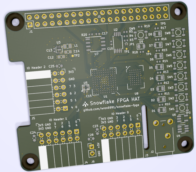
This is a HAT (Raspberry Pi addon board) with an iCE40 HX8k FPGA. The Pi can program the FPGA, and communicate with it via a UART, or a fast, bidirectional SDIO link. This project was spurred by the realisation that Pi 4 is a plausible FPGA development platform: faster processors, expanded memory and, above all, dramatic improvements in Symbiotic EDA's open source design flows in the last few years.
With the exception of the datasheet/ directory (to which I do not lay claim), this repository is distributed under the Apache-2.0 License.
Of the 121 balls on the FPGA's BGA package, I am using 120; the sole unconnected ball is VPP_FAST, which is used only for NVCM programming. This will make the layout exceptionally tight, which is part of the experiment! For a fighting chance, I am using JLCPCB to manufacture the prototype boards, rather than my usual iTead. Their tighter manufacturing tolerances should permit two traces between 0.3 mm pads on a 0.8 mm-pitch BGA, which allows the first 3 ranks of balls to be routed out on layer 1.
The capability requirements for this board are:
This is a 4-layer board.
All layers 1 oz/sqft copper. Assumed stacking for FR4 layers:
These dimensions are not critical. Signal integrity will be improved by minimising separation of L1-L2, but none of the routing is impedance-controlled.
| Qty | Value | Footprint | References |
|---|---|---|---|
| 15 | 100n | Capacitor_SMD:C_0402_1005Metric | C1, C3, C5, C6, C7, C8, C9, C10, C11, C15, C17, C18, C19, C26, C27 |
| 10 | 470 | Resistor_SMD:R_0402_1005Metric | R3, R10, R11, R12, R13, R14, R15, R16, R17, R18 |
| 9 | LED | LED_SMD:LED_0805_2012Metric | D1, D2, D3, D4, D5, D6, D7, D8, D9 |
| 9 | PTS815 | fpga_hat:PTS815 | SW1, SW2, SW3, SW4, SW5, SW6, SW7, SW8, SW9 |
| 6 | 1u | Capacitor_SMD:C_0603_1608Metric | C16, C22, C23, C24, C25, C28 |
| 6 | 4u7 | Capacitor_SMD:C_0603_1608Metric | C2, C4, C12, C14, C20, C21 |
| 5 | TestPoint | fpga_hat:Testpoint_d0.7mm | TP1, TP2, TP3, TP4, TP5 |
| 4 | 100 | Resistor_SMD:R_0402_1005Metric | R1, R2, R8, R9 |
| 3 | 4k7 | Resistor_SMD:R_0402_1005Metric | R4, R5, R19 |
| 3 | Conn_02x06_Top_Bottom | fpga_hat:PinSocket_2x06_P2.54mm_Horizontal | J3, J4, J5 |
| 2 | 220 | Resistor_SMD:R_0402_1005Metric | R6, R7 |
| 1 | 1u | Inductor_SMD:L_0805_2012Metric | L1 |
| 1 | 2x20 | Connector_PinHeader_2.54mm:PinHeader_2x20_P2.54mm_Vertical | J1 |
| 1 | 560p | Capacitor_SMD:C_0402_1005Metric | C13 |
| 1 | 74LVC2G07 | Package_TO_SOT_SMD:SOT-23-6_Handsoldering | U4 |
| 1 | AudioJack3 | fpga_hat:STX-3000_TRS_3.5mm | J2 |
| 1 | CAT24C32WI | Package_SO:TSSOP-8_4.4x3mm_P0.65mm | U2 |
| 1 | Conn_01x02 | Connector_PinHeader_2.54mm:PinHeader_1x02_P2.54mm_Vertical | J6 |
| 1 | DSC60XX | fpga_hat:LGA4_1.6x1.2mm | U5 |
| 1 | IS61WV25616 | fpga_hat:BGA-48_6x8_6.0x8.0mm | U8 |
| 1 | MIC23050-4YML | fpga_hat:DFN8_2x2_0.5mm | U3 |
| 1 | NCP115ASN330T | Package_TO_SOT_SMD:SOT-23-5_HandSoldering | U6 |
| 1 | Solder jumper | fpga_hat:SOLDER_JUMP | JP1 |
| 1 | W25X40CL | Package_SO:SOIC-8_3.9x4.9mm_P1.27mm | U7 |
| 1 | iCE40-HX8k-BG121 | fpga_hat:BGA-121_11x11_9.0x9.0mm | U1 |
The 86 most common of 90 parts.
Wren6991/Snowflake-FPGA
A cheap iCE40 development board, designed on and for Raspberry Pi

Wren6991/RISCBoy
Portable games console, designed from scratch: CPU, graphics, PCB, and the kitchen sink

SepticElectronics/High-Speed-Timer
High Speed Precision Timer 55ps/4ns


MelkhiorVintageComputing/SBusFPGA
Stuff to put a FPGA in a SBus system (SPARCstation)


lrrosa/tia-fpga
FPGA replacement for the Atari 2600 TIA (C010444) video/sound chip, targeting a Sipeed Tang Nano 9K. Open hardware, CERN-OHL-S-2.0.
It measures 65 × 56.5 mm and has 4 copper layers, 1.6 mm thick.
90 parts, built around the ICE40HX8K-BG121TR, 74LVC2G07GV, MIC23050-4YML-TR and CAT24C32WI-GT3. The full list of its parts is on this page, with links to each part's symbol and footprint where PCBKit's library has them.
From the Wren6991/Snowflake-FPGA repository on GitHub, at the commit this page was made from: the board is timelapse/2019-07-03_17:28:54_fpga_hat.kicad_pcb. PCBKit opens the board in the browser, with nothing to install.
Its repository states no licence, so its author keeps all rights: ask Wren6991 before reusing the design.