Skip to the content
PCBKitNew board
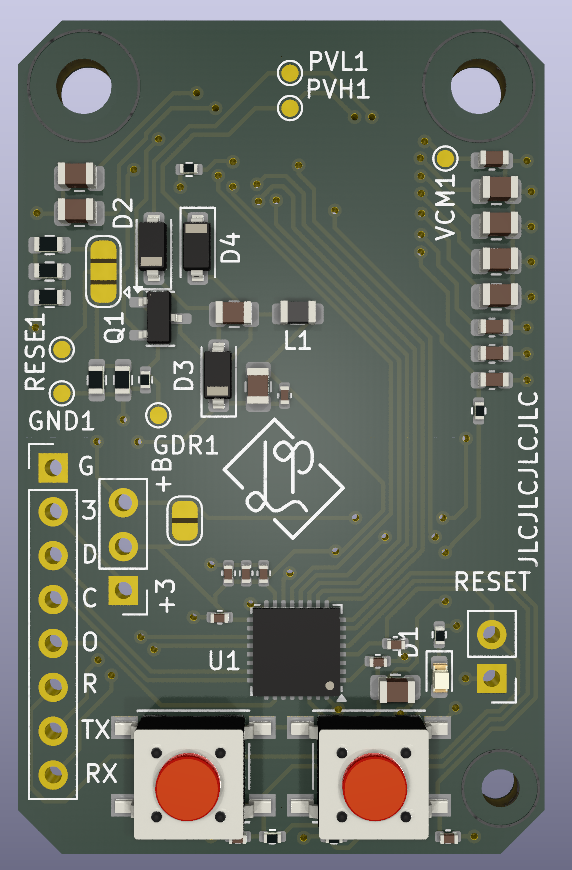
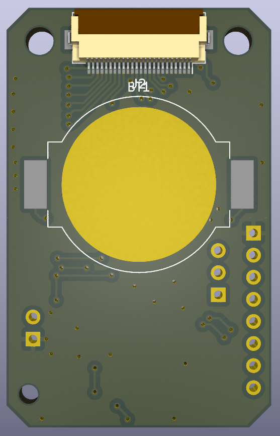
2 layers30.5 × 48.3 mmTama board, the printed circuit board in 3D

Tama board

lprib/tama

E-ink tamagotchi

Size
30.5 × 48.3 mm
Copper layers
2
Thickness
1.6 mm
Parts
58
Nets
55
Pads
185
Tracks, vias
481, 64
Pours
1
Routed
Yes
KiCad
KiCad 9.0 (file 20241229)
Created
20 Apr 2025
Updated
19 May 2025

Overview

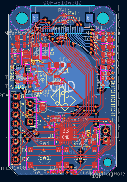
Tama board is an open-source printed circuit board by lprib, from the lprib/tama repository on GitHub. It is a 2-layer board of 30.5 × 48.3 mm with 58 parts on 55 nets, routed with 481 tracks and 64 vias.

It is built around the STM32G431KBU3, MBR0530 and AO3400A. Its parts include 22 capacitors, 11 resistors, 4 diodes, 2 connectors and 2 switches. It belongs with the STM32 boards of this library.

Main components

3

README

README.md

Tamagotchi

Design of an E-Ink tamagotchi board thing that runs off a CR2032 coin cell battery. Uses a GDEW0154M09 E-Ink 1.5x1.5in display from GoodDisplay.

top bottom layout Layout is a bit messy about breaking ground plane and having shit VDD distribution, but it should be good enough :^).

Notes

MCU Selection

Final choice

STM32G431

  • 128Kb flash enough for bitmaps
  • ultra low power consumption is STANDBY or SHUTDOWN
  • Tiny package to fit on PCB (QFN32)

Requirements

  • ultra low power
  • 1x SPI
  • bitmap ROM
    • display is 200x200 pixels, 5kB for full image, maybe 3kB conservative for run length encoded image?
    • Want at least 10 images, so 30kB ROM required

Going for only JLCPCB approved parts or minimal extended parts

For STM, this is:

  • STM32 F103
    • RUN 8MHz 8.6mA all peripherals
    • RUN 8MHz 6.8mA no peripherals (closer to reality)
    • STANDBY 3.2uA
  • STM32 L151 (no stock)
  • STM32 F030
    • RUN 8MHz 4.4mA
    • STANDBY ~3uA
  • STM32 G030
    • internal HSI oscillator
    • 64kB flash / 8k ram
    • RUN 1.3mA
    • STANDBY 1.4uA
  • STM32 G431
    • 128Kb flash (no external memory needed)
    • RUN 8MHz 1.10mA
    • RUN 1MHz 0.2mA
    • STANDBY 175nA
    • SHUTDOWN mode (no RTC): 74nA
    • SHUTDOWN mdoe (RTC via external 32k xtal) : 0.5/0.7uA
      • Guess this included the power draw of the crystal
  • STM8 S105K6T6
    • 32kB flash
    • 2kB ram
    • External EEPROM required for bitmaps?
  • STM8 S003F3P6
    • 8kB flash
    • 1kB ram

G431

F103

Heaps of stock and 10 year guarantee At minimum core speed 8MHz

  • STOP mode retains ram and registers
    • wake up with EXTI pin
    • wakeup with WKUP pin
    • wakeup with RTC alarm
    • 3.2 uA (DECENT)

L151

** Not for new designs **

** JLC stock 1 (!) **

  • 214 μA/MHz Run mode
  • 9 μA Low-power run mode
  • 1.2 μA Stop mode + RTC
  • 0.9 μA Standby mode + RTC
  • 0.3 μA Standby mode (3 wakeup pins)

Modes:

  • Sleep
    • core stopped, peripheral can intterrupt/wakeup
  • Low power run
    • core clocked at 65KHz
  • Stop mode with RTC
    • RAM and registers preserved, wakeup via EXTI pin
    • wakeup with RTC timestamp (or without RTC
  • Standby mode
    • Ram and regists lost
    • wakeup with external reset NST
    • wakeup rising edge of one of the three WKUP pins
    • wakeup on RTC alarm

Display

5x GDEW0154M09

Battery / Power

MCU

  • worst cast STM32G431\
  • core
    • RUN 8MHz 1.10mA
    • RUN 26MHz 3.2mA (maximum of Range 2 PLL freqs)
  • periph
    • FLASH 4.6uA/mHZ
    • GPIOA 0.73uA/mHZ
    • GPIOB 0.41uA/mHZ
    • SPI1 1.92uA/MHz
    • RTC 2.92uA/MHz
    • AHB bus matrix 4.07uA/MHz
    • AHB to APB1 bridge 0.32
    • AHB to APB2 bridge 0.30 TOTAL peripheral
    • 394uA at 26MHz
      TOTAL
    • 3.6mA RUNNING
    • 0.7uA SHUTDOWN

Screen

  • Image update max 3mA RUNNING
  • Standby panel 5uA SHUTDOWN

Battery

  • 235 mAh to 2v (require boost converter)
  • screen minimum supply voltage 2.3V
  • MCU minimum supply voltage 1.7V
  • At 2.3V, this gives about 200mAH of usable longevity from the coin cell

Totals

Assuming 100% boost convert efficiency (haha)

  • RUNNING 6.6mA
    • 35 hours
  • STANDBY 6uA
    • 4 years 3 weeks :^)

PCB assembly

Went relatively smoothly except

  • U1 (STM32 ended up rotated 90 degrees counter clockwise from its desired position). Changed rotation from 180 to 90.
  • Q1 (Sot23 mosfet) ended up 180 degrees out. Changed from 0 to 180
  • D1 footprint was fucked because I got confused by the example footpint from the website.
    • Couldn't be bothered to regenerate and re-do order with new gerbers so just rotated the pick-and-place position of the diode without changing silkscreen etc.
    • JLC realized and tried to fix it by rotating it to the silkscreen-defined position, told them to put it back to the (seemingly incorrect) position.

Parts

58
QtyValueFootprintReferences
84.7u 25VCapacitor_SMD:C_0805_2012MetricC10, C11, C12, C14, C15, C17, C18, C21
6TestPointTestPoint:TestPoint_Pad_D1.0mmGDR1, GND1, PVH1, PVL1, RESE1, VCM1
51RResistor_SMD:R_0603_1608MetricR7, R8, R9, R10, R11
4100nCapacitor_SMD:C_0402_1005MetricC1, C2, C4, C7
41u 50VCapacitor_SMD:C_0603_1608MetricC16, C19, C20, C22
310nCapacitor_SMD:C_0402_1005MetricC5, C8, C9
31MResistor_SMD:R_0402_1005MetricR1, R2, R6
3MBR0530Diode_SMD:D_SOD-123D2, D3, D4
2MountingHoleMountingHole:MountingHole_3.2mm_M3H1, H2
2SW_PushButton_Switch_SMD:SW_SPST_PTS645SW1, SW2
1100KResistor_SMD:R_0402_1005MetricR4
1100RResistor_SMD:R_0402_1005MetricR3
110RResistor_SMD:R_0402_1005MetricR5
110uCapacitor_SMD:C_0402_1005MetricC13
110uHInductor_SMD:L_0805_2012MetricL1
11uCapacitor_SMD:C_0402_1005MetricC6
14.7uCapacitor_SMD:C_0805_2012MetricC3
1AO3400APackage_TO_SOT_SMD:SOT-23-3Q1
1BatteryBattery:BatteryHolder_MPD_BC2003_1x2032BT1
1Conn_01x08_PinConnector_PinHeader_2.54mm:PinHeader_1x08_P2.54mm_VerticalJ1
1GDEW0154M09Connector_FFC-FPC:Hirose_FH12-24S-0.5SH_1x24-1MP_P0.50mm_HorizontalJ2
1LEDLED_SMD:LED_0603_1608MetricD1
1MountingHoleMountingHole:MountingHole_2.2mm_M2H3
1PERMANENT BATTERY SELECTJumper:SolderJumper-2_P1.3mm_Open_RoundedPad1.0x1.5mmJP3
1POWER SOURCE SELECTConnector_PinHeader_2.54mm:PinHeader_1x03_P2.54mm_VerticalJP1
1RESETConnector_PinHeader_2.54mm:PinHeader_1x02_P2.54mm_VerticalJP2
1RESISTANCE SELECTJumper:SolderJumper-3_P1.3mm_Open_RoundedPad1.0x1.5mmJP4
1STM32G431KBU3Package_DFN_QFN:QFN-32-1EP_5x5mm_P0.5mm_EP3.45x3.45mmU1

Questions

How big is the Tama board PCB?

It measures 30.5 × 48.3 mm and has 2 copper layers, 1.6 mm thick.

What parts does the Tama board use?

58 parts, built around the STM32G431KBU3, MBR0530 and AO3400A. The full list of its parts is on this page, with links to each part's symbol and footprint where PCBKit's library has them.

Where can I download the Tama board KiCad files?

From the lprib/tama repository on GitHub, at the commit this page was made from: the board is tama_board/tama_board.kicad_pcb and its schematic tama_board/tama_board.kicad_sch. PCBKit opens the board in the browser, with nothing to install.

Can I use the Tama board design in my own project?

Its repository states no licence, so its author keeps all rights: ask lprib before reusing the design.

Similar boards

  • 2 layers49.6 × 43.6 mmA1-Toolhead Board, the printed circuit board in 3D

    A1-Toolhead Board

    DevCyclonekitten/Bambu-A1-Klipper

    A repository about the development of modifying a bambu labs a1 printer to run on klipper

    74 parts4GPL-3.0
  • 4 layers49.8 × 25.5 mmCorevus toolboard, the printed circuit board in 3D

    Corevus toolboard

    calithameridi/corevus

    High-flexibility, low-cost mechatronics controller for 3D printers

    84 parts25
  • 4 layers36.5 × 69 mmStorm tracker, the printed circuit board in 3D

    Storm tracker

    solderable/storm-tracker-hardware

    Open-source-ready Storm Tracker hardware design, documentation, BOM, and manufacturing package

    102 parts58
  • 2 layers33.8 × 46 mmWatchy, the printed circuit board in 3D

    Watchy

    xywatch/watchy-hardware-v2

    watchy hardware v2 with typec

    64 parts8
  • 2 layers84 × 98 mmFalloutbadge, the printed circuit board in 3D

    Falloutbadge

    sophiayduan/badges

    hackathon pcb badges

    93 parts3Unlicense
  • 2 layers61.7 × 35.1 mmMS88SF2 eInk display v2, the printed circuit board in 3D

    MS88SF2 eInk display v2

    chacal/pcbs

    Hardware design files for various hobby projects

    61 parts1MIT
  • 4 layers66.5 × 50.7 mmCtc 2025, the printed circuit board in 3D

    Ctc 2025

    challengethecyber/ctf-2025-badge

    66 parts1MIT
  • 2 layers83.1 × 56.2 mmSchematics, the printed circuit board in 3D

    Schematics

    fulvionardi/Epaper

    This project is a replication of the Waveshare 3.6inch e-Paper HAT+ schematics, originally documented in 3.6inche-PaperHAT+Schematics.pdf.

    73 parts1