


2 layers368.3 × 215.9 mm

 lfantoniosi/CoCoTANG12
CoCoTANG upgrades the Radio Shack/Tandy Color Computer with a Tang Nano 20K FPGA board and CoCo 3 video and memory features.
CoCoTANG is an open-source printed circuit board by lfantoniosi, from the lfantoniosi/CoCoTANG repository on GitHub. It is a 2-layer board of 236.8 × 129.1 mm with 127 parts on 213 nets, routed with 3,403 tracks and 309 vias.
It is built around the 74LVC245AD, 74HCT245 and 74HC139D, with the 74HCT11D, 74HCT138D and 74HCT30D among its other parts. Its parts include 32 resistors, 27 capacitors, 25 connectors, 18 ICs and 9 transistors.


CoCoTANG upgrades the Radio Shack/Tandy Color Computer with a Tang Nano 20K FPGA board and CoCo 3 video and memory features. It retains the MC6809E CPU and motherboard PIAs while the FPGA implements the GIME video and memory subsystem, HDMI and analog video outputs, and a Glenside-compatible IDE interface backed by a microSD card. It also provides 8 MB of RAM, Orchestra-90 audio with stereo over HDMI, and Tandy Speech/Sound Cartridge (SSC) support.
This repository contains the FPGA sources, KiCad designs, fabrication files, and bill of materials.
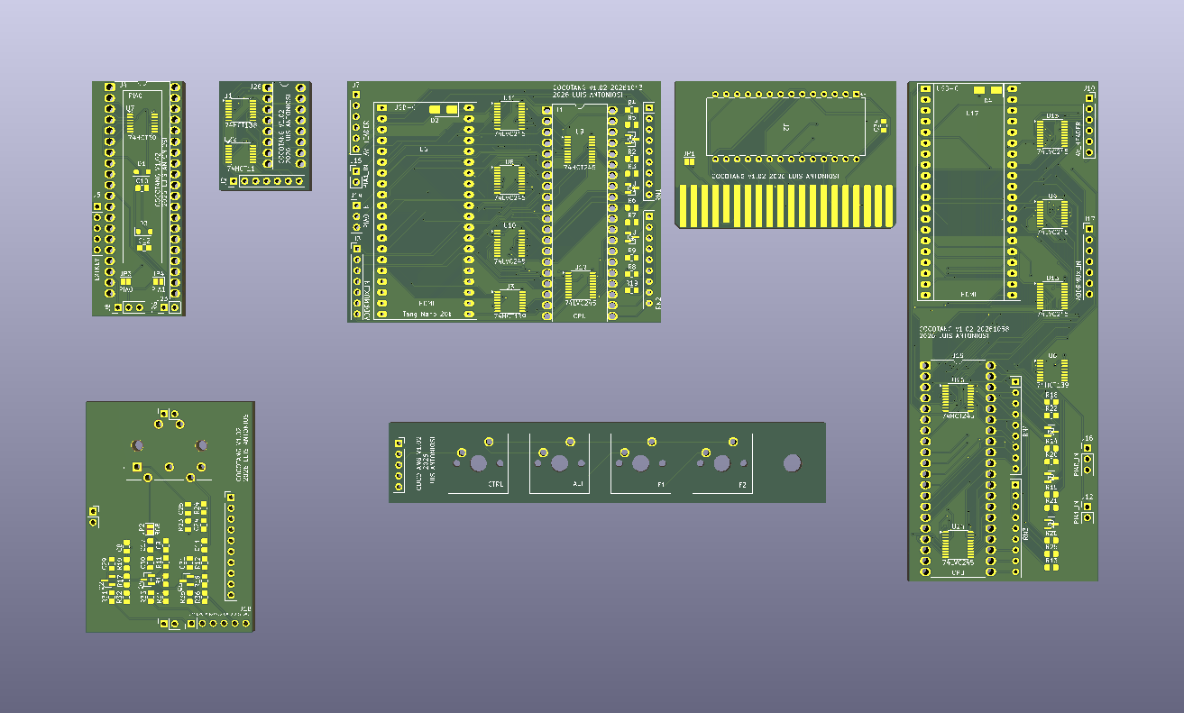
The assembly uses a main board for the CPU and Tang Nano 20K, PIA0 and PIA1 adapter boards, and an address mux board that replaces the motherboard 74LS138. An analog video hat and an HDB-DOS ROM cartridge are optional. The render above shows the boards arranged as a PCB panel. HDB-DOS can also be supplied through an FD-502 ROM socket or CoCo SDC flash bank.
The design uses NTSC machine clocking. The GIME's 50 Hz setting remains available, but selecting it does not switch to a PAL crystal. PAL-encoded CVBS/S-Video output is also supported. See Build on macOS or Linux for video targets and the FPGA pin and bus map for hardware connections.
So far, The Contras is the only game found to fail to load in its original form. CoCoTANG's 262.5-scanline timing drifts relative to the original CoCo 3. The resulting timing difference affects an unprotected code section in the game and prevents the original version from loading.
Use the patched version of The Contras instead. This patched version also includes keyboard enhancements.
A Multi-Pak Interface (MPI) holds the cartridge data bus in a way that prevents access to CoCoTANG's internal peripheral registers. With an MPI connected, the internal Glenside IDE, SSC sound/speech, and Orchestra-90 are unavailable. Software that uses these internal devices must be run without the MPI.
An MPI is required to use real floppy drives. Plug the floppy disk controller into the MPI and connect the drives to that controller. This setup uses the external floppy controller, with the internal IDE, SSC, and Orchestra-90 unavailable as described above.
| Item | File or notes |
|---|---|
| PCB fabrication files | Gerber/drill ZIPs for each board |
| KiCad schematic and PCB | kicad/ |
| Components | Full bill of materials below |
| FPGA project and sources | fpga/ |
| FPGA pin/bus map | fpga/docs/pinout.md |
For one CoCoTANG installation, you need one main board, one address mux board, and two PIA boards: one for PIA0 and one for PIA1. There are two main-board versions, for motherboard revisions 20261043 and 20261058; choose the version that matches your motherboard. The HDB-DOS cartridge and video hat are optional.
| Board | Quantity per installation | Gerber/drill ZIP |
|---|---|---|
| Main board (CPU / Tang Nano 20K) | 1 required; choose the matching version | See the compatibility table below |
| Address mux (addrmux) | 1 required | gerber_addrmux.zip |
| PIA card | 2 required: PIA0 and PIA1 | gerber_pia.zip |
| HDB-DOS cartridge | 1 optional | gerber_cart.zip |
| Video hat | 1 optional | gerber_avideo.zip |
| External keyboard extension | 1 optional | gerber_extkey.zip |
Use the same PIA Gerber ZIP to fabricate both PIA cards. Upload each desired board's ZIP separately to your PCB manufacturer and select the quantities above, subject to the manufacturer's minimum order quantity.
Select 1.2 mm PCB thickness when ordering the adapter boards. The thinner boards reduce the installed profile and help the assembly fit under the keyboard.
Tandy used several motherboard layouts for the CoCo 2. Identify your motherboard before ordering boards: the CPU and address mux adapters must fit its layout. Only the revisions marked compatible below are currently supported; other layouts may need different adapters.
| Motherboard revision | Compatible | Main board Gerber ZIP |
|---|---|---|
| 20261043 | Yes | gerber_main_20261043.zip |
| 20261058 | Yes | gerber_main_20261058.zip |
| 20261044 | No | — |
| 20261045 | No | — |
| 20261059 | No | — |
CoCo 1 compatibility has not yet been tested.
Both main-board versions (20261043 and 20261058) use the same components and quantities; only the PCB layout differs. Use the fabrication drawing and silkscreen for the version you are assembling.
Use HCT parts for the 5 V logic: U9/U16 (74HCT245, depending on the main-board version), U1 (74HCT138), U22 (74HCT11), and U7 (74HCT30). Their TTL-compatible inputs accept the logic levels used at the motherboard interface. The table below gives the manufacturer part numbers, matching DigiKey part numbers, and TSSOP packages.
U3/U6 are 74HC139 decoders powered from 3.3 V, with their select inputs driven by the FPGA. Keep the HC version here: 74HCT139 is specified for a 4.5–5.5 V supply. A 3.3 V supply makes HC139 suitable for this 3.3 V logic domain; it does not turn HC into a generally TTL-compatible family. The KiCad labels now identify both decoder instances as HC139.
The four 74LVC245 buffers on each main board remain LVC parts for the 3.3 V interface; their reference designators are listed for both layouts below. Their TSSOP ordering code is SN74LVC245APWR.
The reference columns identify the same components on each layout. Lists follow the same order across both columns. The three interrupt/reset resistors and the additional R/W pull-up are listed separately. The other adapter boards below are shared between both versions.
| Qty | Value | Description | DigiKey P/N | 20261043 references | 20261058 references | Alternative link |
|---|---|---|---|---|---|---|
| 1 | Tang Nano 20K | Tang Nano 20K FPGA Board | N/A | U5 | U17 | AliExpress |
| 6 | 0.1 µF | CAP CER 0805 0.1UF 100VDC X7R | 399-C0805F104K1RACAUTOCT-ND | C2, C3, C4, C5, C6, C7 | C13, C16, C19, C14, C18, C15 | |
| 3 | MMBT3904-TP | TRANS NPN 40V 0.2A SOT-23 | MMBT3904TPMSCT-ND | Q7, Q8, Q9 | Q1, Q3, Q6 | |
| 1 | SS14 | DIODE SCHOTTKY 40V 1A DO214AC | SS14CT-ND | D2 | D4 | |
| 3 | 10K | RES 10K OHM 1% 1/8W 0805 | 311-10.0KCRCT-ND | R2, R4, R6 | R14, R18, R15 | |
| 3 | 4.7K | RES 4.7K OHM 1% 1/8W 0805 | 311-4.70KCRCT-ND | R3, R5, R7 | R20, R22, R21 | |
| 1 | 4.7K | R/W pull-up, 1% 1/8W 0805 | 311-4.70KCRCT-ND | R19 | R13 | |
| 2 | 47K | RES SMD 47K OHM 1% 1/8W 0805 | YAG3735CT-ND | R8, R9 | R25, R26 | |
| 2 | 4.7K | RES ARRAY 8 RES 4.7K OHM 9SIP | 4609X-101-472LF-ND | RN1, RN2 | RN4, RN3 | |
| 4 | SN74LVC245APWR | 8-bit bus transceiver, 1.65–3.6 V, TSSOP-20 | 296-1233-1-ND | U8, U10, U11, U12 | U4, U13, U15, U14 | |
| 1 | SN74HCT245PWR | 8-bit bus transceiver, TTL inputs, 4.5–5.5 V, TSSOP-20 | 296-8404-1-ND | U9 | U16 | |
| 1 | 74HC139PW,118 | Dual 2-to-4 decoder, CMOS inputs, 2–6 V; used at 3.3 V, TSSOP-16 | 1727-6580-1-ND | U3 | U6 | |
| 1 | SIL FEMALE HDR | MACHINE PIN SOCKET 40P 2.54MM PI | SMC-1A-40-1-GT-HT | U5 | U17 | AliExpress |
| 1 | DIP-40 SOCKET | MACHINE PIN SOCKET, IC, DIP, 40P | ICM-640-1-GT-HT | J1 | J19 | AliExpress |
| Qty | Value | Description | DigiKey P/N | References | Alternative link |
|---|---|---|---|---|---|
| 1 | 0.1 µF | CAP CER 0805 0.1UF 100VDC X7R | 399-C0805F104K1RACAUTOCT-ND | C1 | |
| 1 | DIP-40 SOCKET | MACHINE PIN SOCKET, IC, DIP, 40P | ICM-640-1-GT-HT | J4 | AliExpress |
| 1 | 74HCT30PW,118 | 8-input NAND gate, TTL inputs, 4.5–5.5 V, TSSOP-14 | 1727-6632-1-ND | U7 | |
| 2 | 1,800 pF | CAP CER 1800PF 250V C0G/NP0 0805 | 490-GCM21A5C2E182FX01DCT-ND | C10,C12 | |
| 2 | SD103BW | DIODE SCHOTTKY 30V 0.35A SOD123F | 4878-SD103BWCT-ND | D1,D3 |
| Qty | Value | Description | DigiKey P/N | References | Alternative link |
|---|---|---|---|---|---|
| 1 | DIP-40 SOCKET | MACHINE PIN SOCKET, IC, DIP, 40P | ICM-640-1-GT-HT | J4 | AliExpress |
| Qty | Value | Description | DigiKey P/N | References | Alternative link |
|---|---|---|---|---|---|
| 2 | 0.1 µF | CAP CER 0805 0.1UF 100VDC X7R | 399-C0805F104K1RACAUTOCT-ND | C32,C33 | |
| 1 | SN74HCT138PWR | 3-to-8 decoder, TTL inputs, 4.5–5.5 V, TSSOP-16 | 296-8388-1-ND | U1 | |
| 1 | 74HCT11PW,118 | Triple 3-input AND gate, TTL inputs, 4.5–5.5 V, TSSOP-14 | 1727-7964-1-ND | U22 | |
| 1 | DIP-16 SOCKET | CONN IC DIP SOCKET 16POS GOLD | SA163000 | J28 | AliExpress |
| Qty | Value | Description | DigiKey P/N | References | Alternative link |
|---|---|---|---|---|---|
| 1 | DIP-28 SOCKET | CONN IC DIP SOCKET 28POS GOLD | 110-41-628-41-001000 | U2 | AliExpress |
| 1 | 0.1 µF | CAP CER 0805 0.1UF 100VDC X7R | 399-C0805F104K1RACAUTOCT-ND | C34 | |
| 1 | AT28C64B-15PU | IC EEPROM 64KBIT PARALLEL 28DIP | AT28C64B-15PU-ND | U2 |
| Qty | Value | Description | DigiKey P/N | References | Alternative link |
|---|---|---|---|---|---|
| 3 | 0.1 µF | CAP CER 0805 0.1UF 100VDC X7R | 399-C0805F104K1RACAUTOCT-ND | C29,C30,C31 | |
| 3 | 470 pF | CAP CER 470PF 50V C0G/NP0 0805 | 490-1617-1-ND | C8,C9,C11 | |
| 1 | 1 µF | CAP CER 1UF 25V X7R 0805 | 399-C0805C105K3RACTUCT-ND | C15 | |
| 6 | 1K | RES 1K OHM 1% 1/8W 0805 | 541-3977-1-ND | R31,R17,R33,R1,R35,R16 | |
| 3 | 75 | RES 75 OHM 1% 1/8W 0805 | 541-CRCW080575R0FKEACCT-ND | R10,R11,R12 | |
| 3 | 4.7K | RES 4.7K OHM 1% 1/8W 0805 | 311-4.70KCRCT-ND | R32,R34,R36 | |
| 1 | 6.8 nF | CAP CER 6800PF 250V C0G/NP0 0805 | 490-GCM21B5C2E682JX0ALCT-ND | C24 | |
| 1 | 4.7 µF | CAP CER 4.7UF 16V X7R 0805 | 732-7666-1-ND | C25 | |
| 1 | 100K | RES 100K OHM 1% 1/8W 0805 | 541-3978-1-ND | R24 | |
| 3 | MMBT3904-TP | TRANS NPN 40V 0.2A SOT-23 | MMBT3904TPMSCT-ND | Q2,Q4,Q5 | |
| 1 | DIN-5 FEMALE | D5 PIN DIN SOCKET 180 DEGREE | 4654-FC680805-ND | J24 | AliExpress |
| Qty | Value | Description | DigiKey P/N | References | Alternative link |
|---|---|---|---|---|---|
| 2 | PRPC040SBAN-M71RC | CONN HEADER R/A 40POS 2.54MM | S1111EC-40-ND | ||
| 1 | 1950 | JUMPER WIRE F TO F 6" 28AWG | 1528-1961-ND |
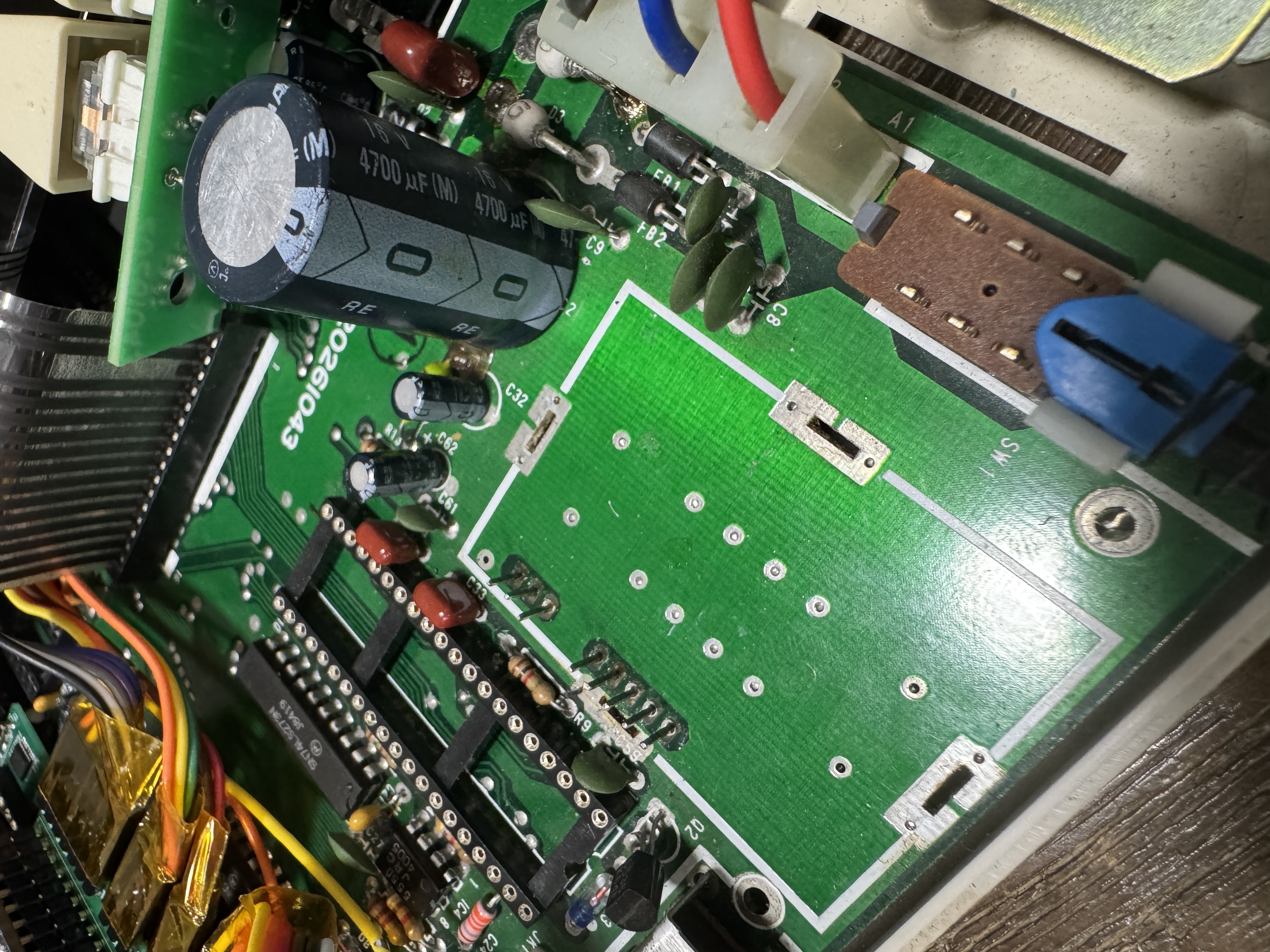
Print the fabrication drawing and use it with the board silkscreen to identify component positions. Check diode orientation before soldering. The main-board bill of materials applies to both supported versions; component positions differ between layouts.
Several adapters have oversized socket holes. They require machined-pin sockets whose pins extend through the adapter to connect to the motherboard socket while holding the original IC above it. Use 1.2 mm PCBs to reduce the overall assembly height and improve clearance under the keyboard.
104 are oversized, and nearby radial capacitors may also interfere. Where necessary, desolder and reposition their leads before bending the capacitors closer to the motherboard..fs bitstream and CoCo 3 ROM, following the programming instructions below.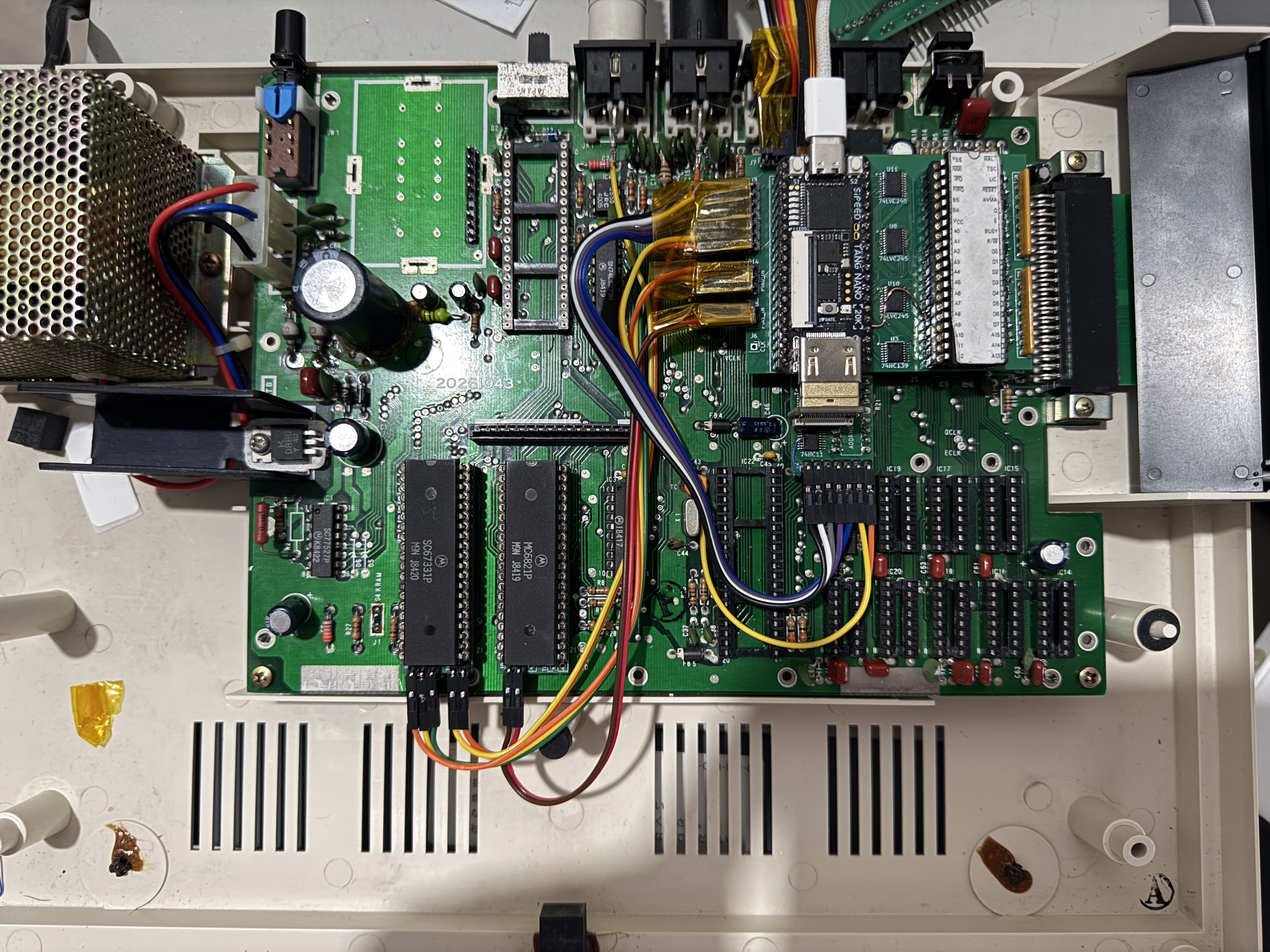
The photos below show the component population and header placement, in assembly order. Front and back views are included where available.
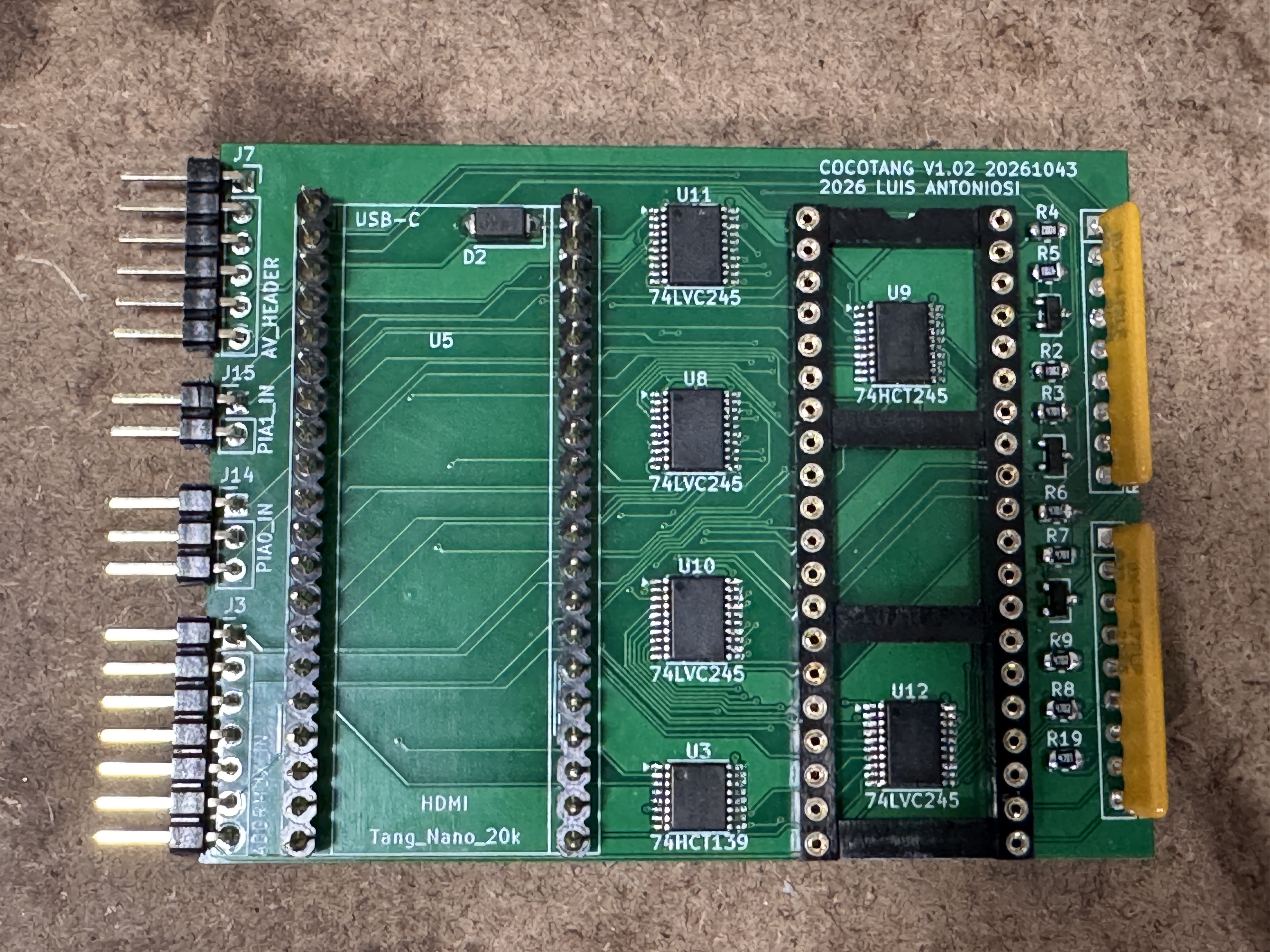
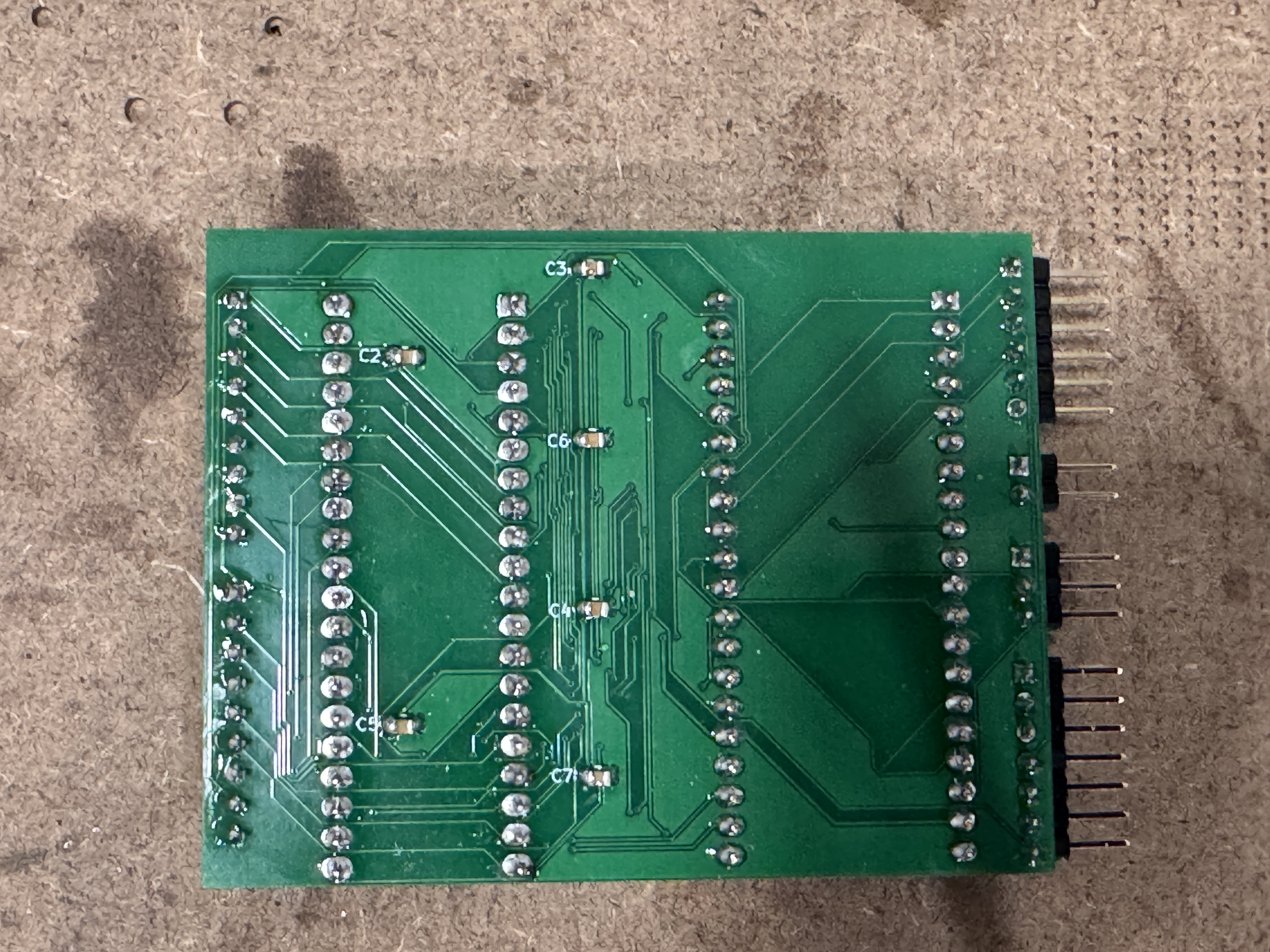
The main board carries the CPU socket, Tang Nano 20K headers, bus buffers, and connections to the other adapters. The photos show the assembled board before fitting the CPU and FPGA module. Choose the layout that matches your motherboard revision.
| Front | Back |
|---|---|
 |  |
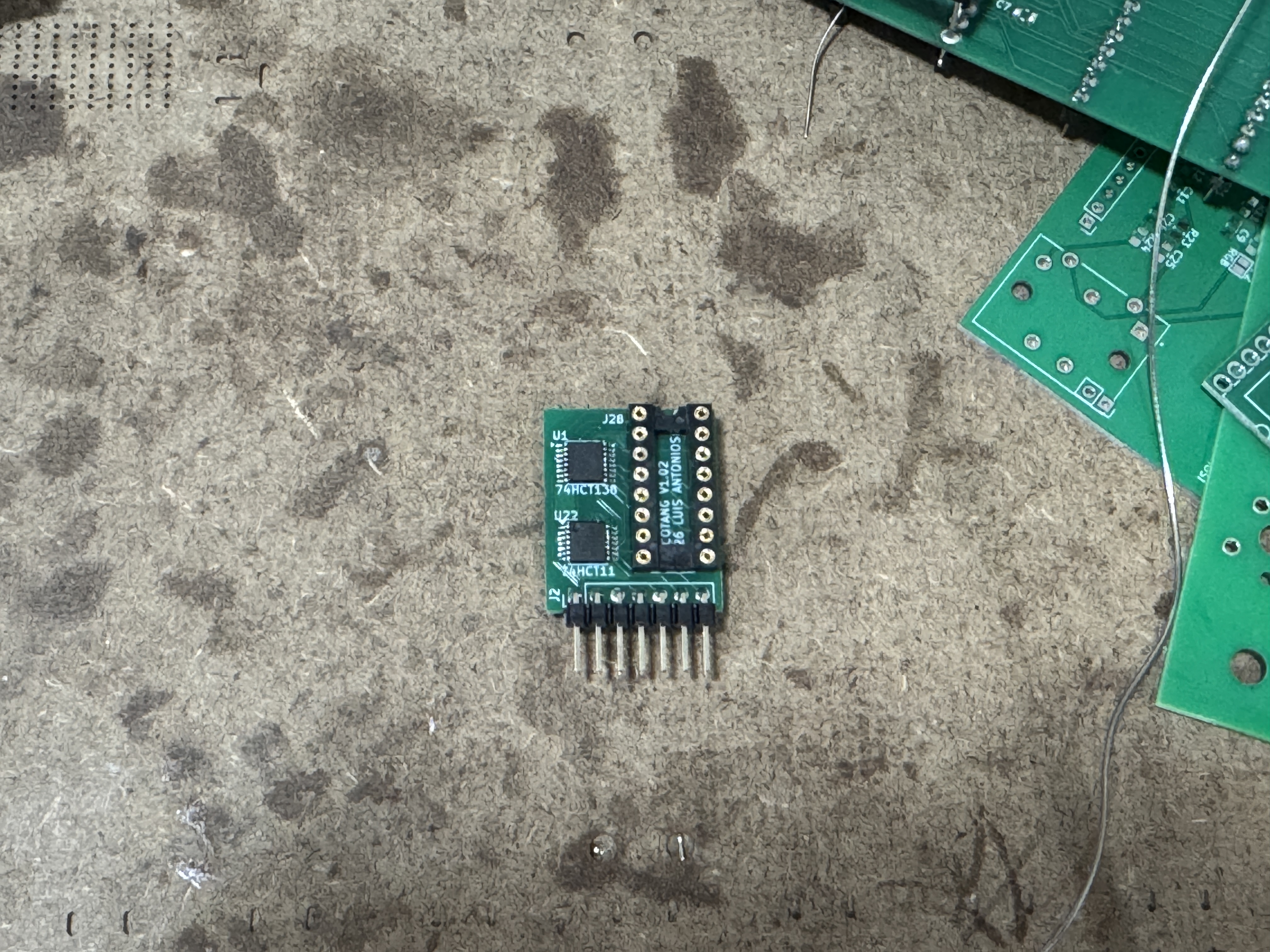
The address mux adapter plugs into the motherboard's former 74LS138 position and connects to the main board. Leave the 74LS138 socket on the ADDRMUX adapter empty; do not reinstall the original IC in it. The adapter's onboard logic replaces its function.
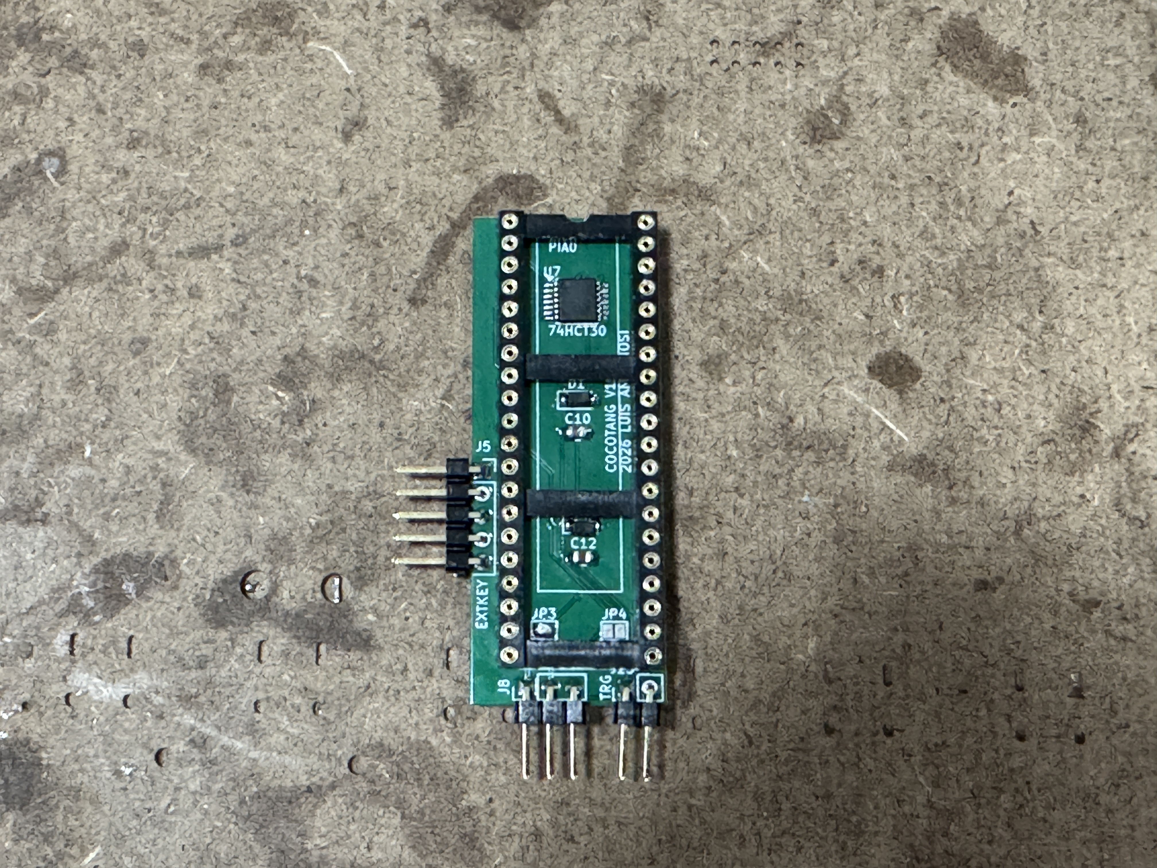
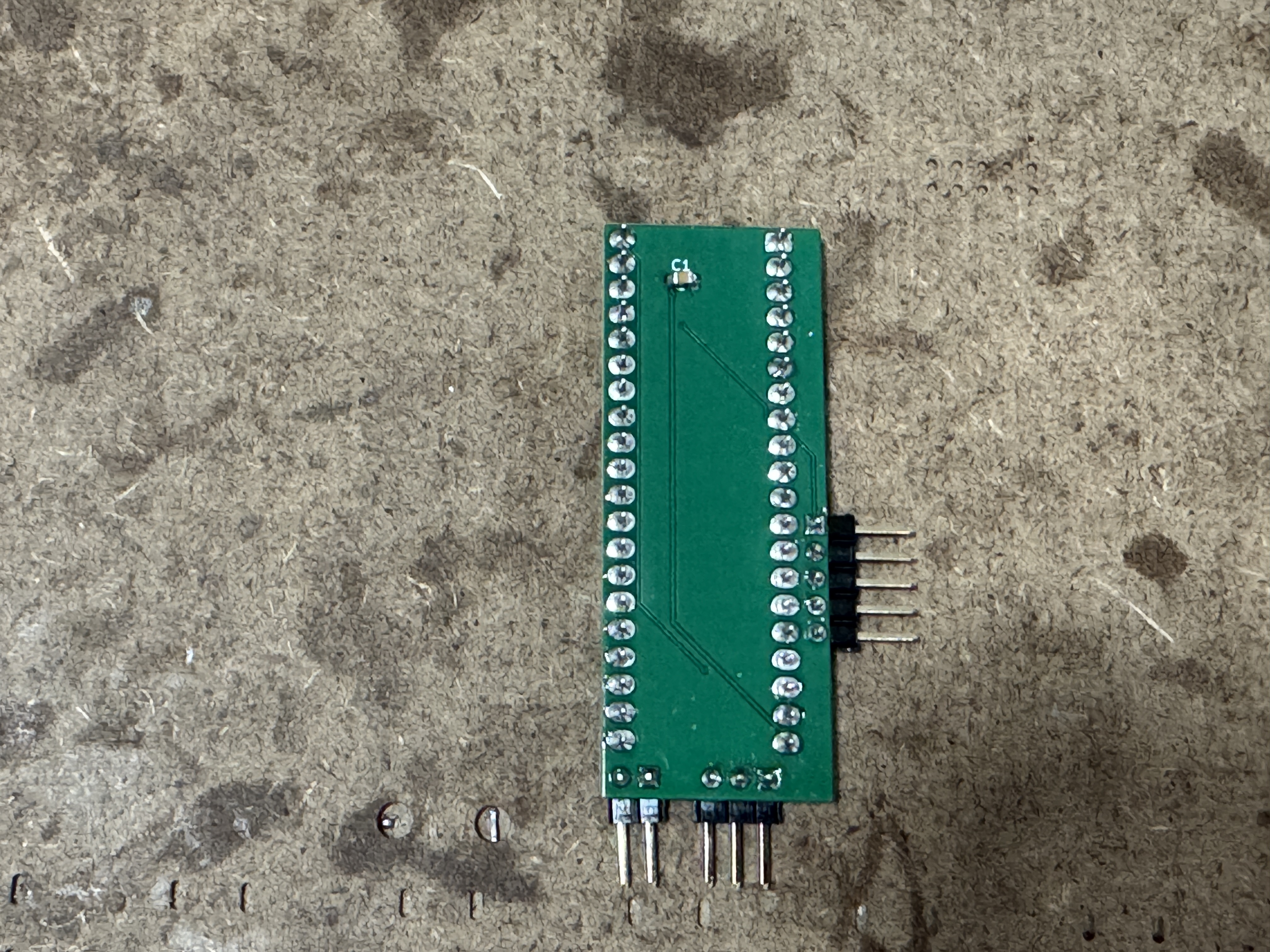
Populate the logic IC, diodes, capacitors, and headers required for PIA0, and select the PIA0 jumper setting. The external keyboard header is fitted only on this adapter. These photos show the board before installing the PIA.
| Front | Back |
|---|---|
 |  |
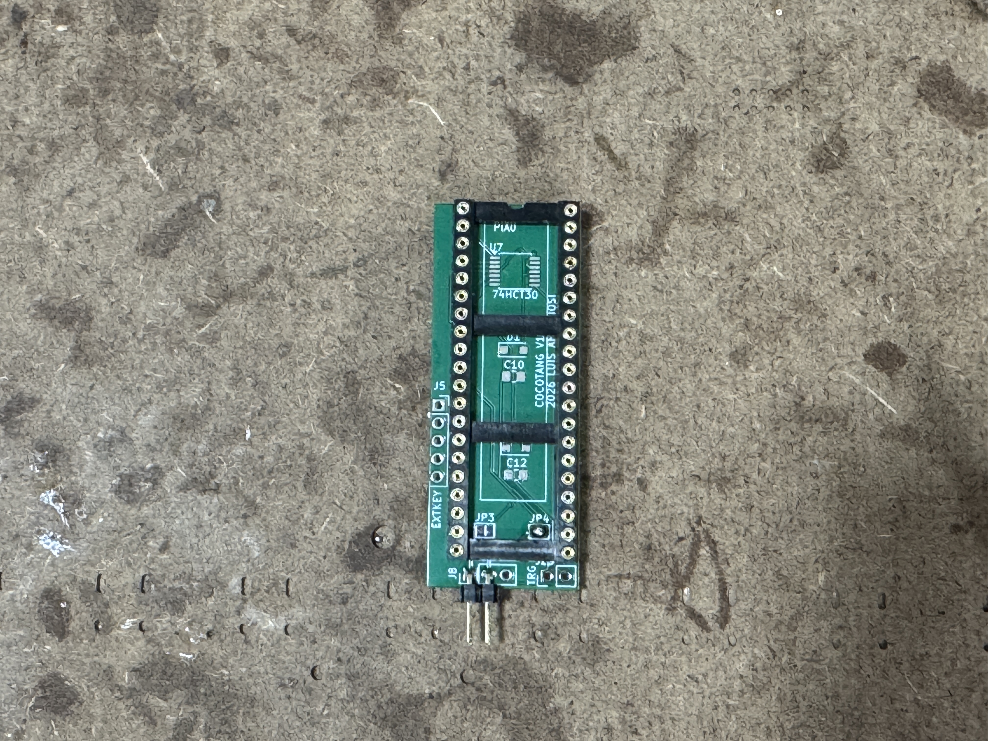
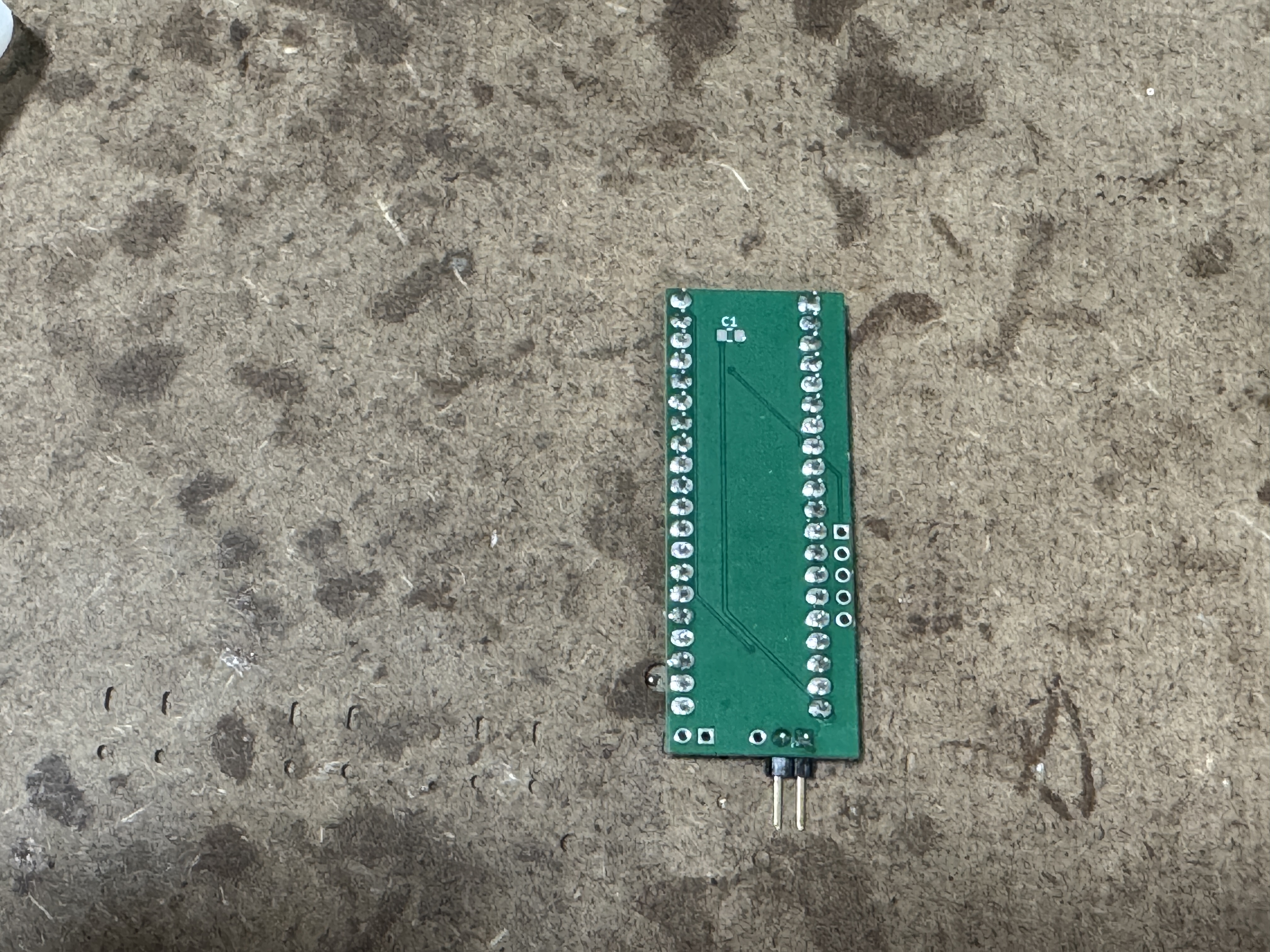
PIA1 uses the same PCB with the PIA1 jumper setting. Fit the socket and required signal header; leave the PIA0-only logic, diodes, capacitors, and external keyboard header unpopulated. These photos show the board before installing the PIA.
| Front | Back |
|---|---|
 |  |
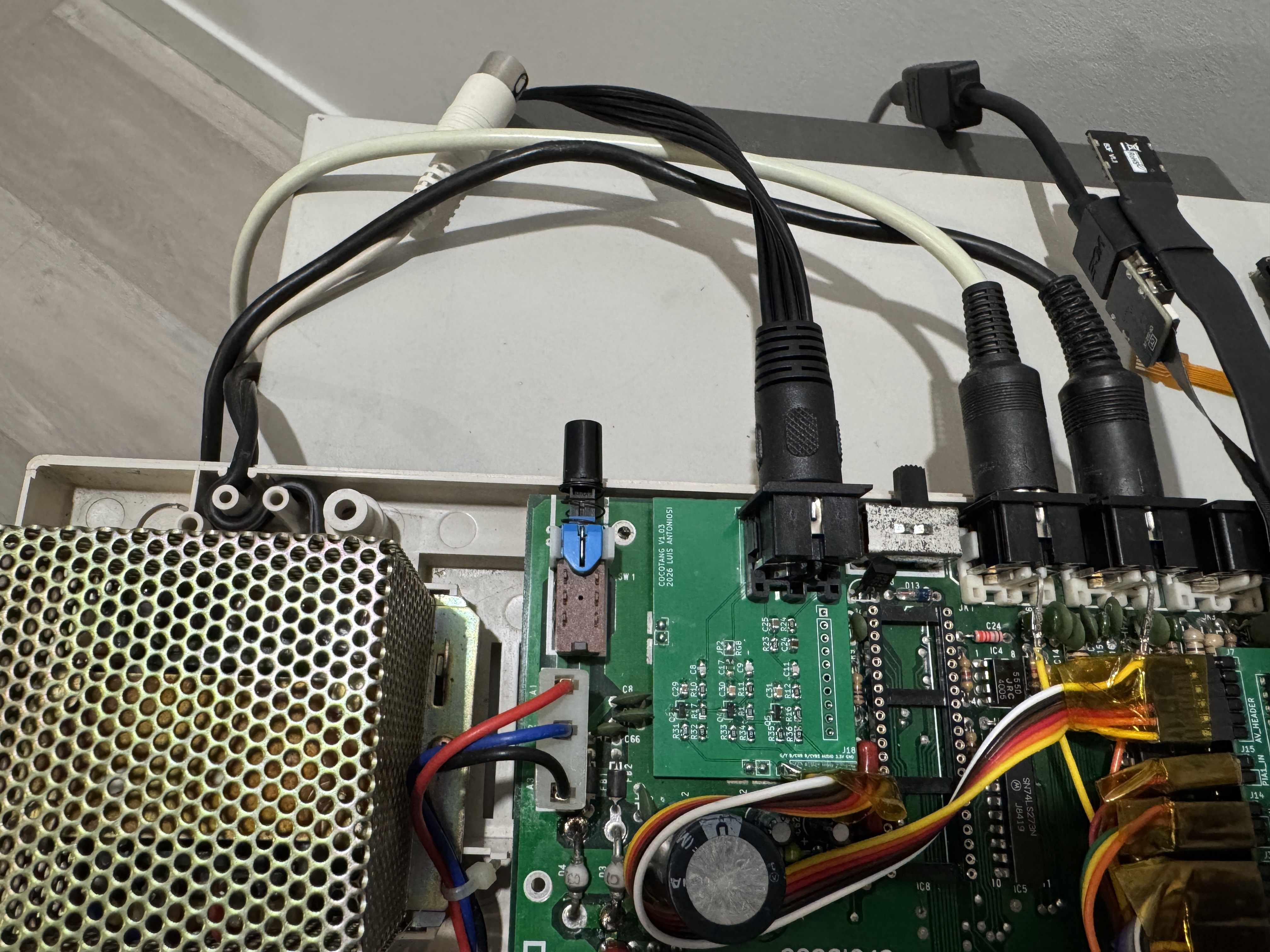
The optional analog audio/video board can be mounted in the original RF modulator/shield location. Enlarge the opening in the CoCo's cover to clear the 5-pin DIN connector. Use pin headers on the back of the AVIDEO PCB to secure it to the CoCo motherboard, as shown in the back view.
| Front | Back / mounting headers |
|---|---|
 | 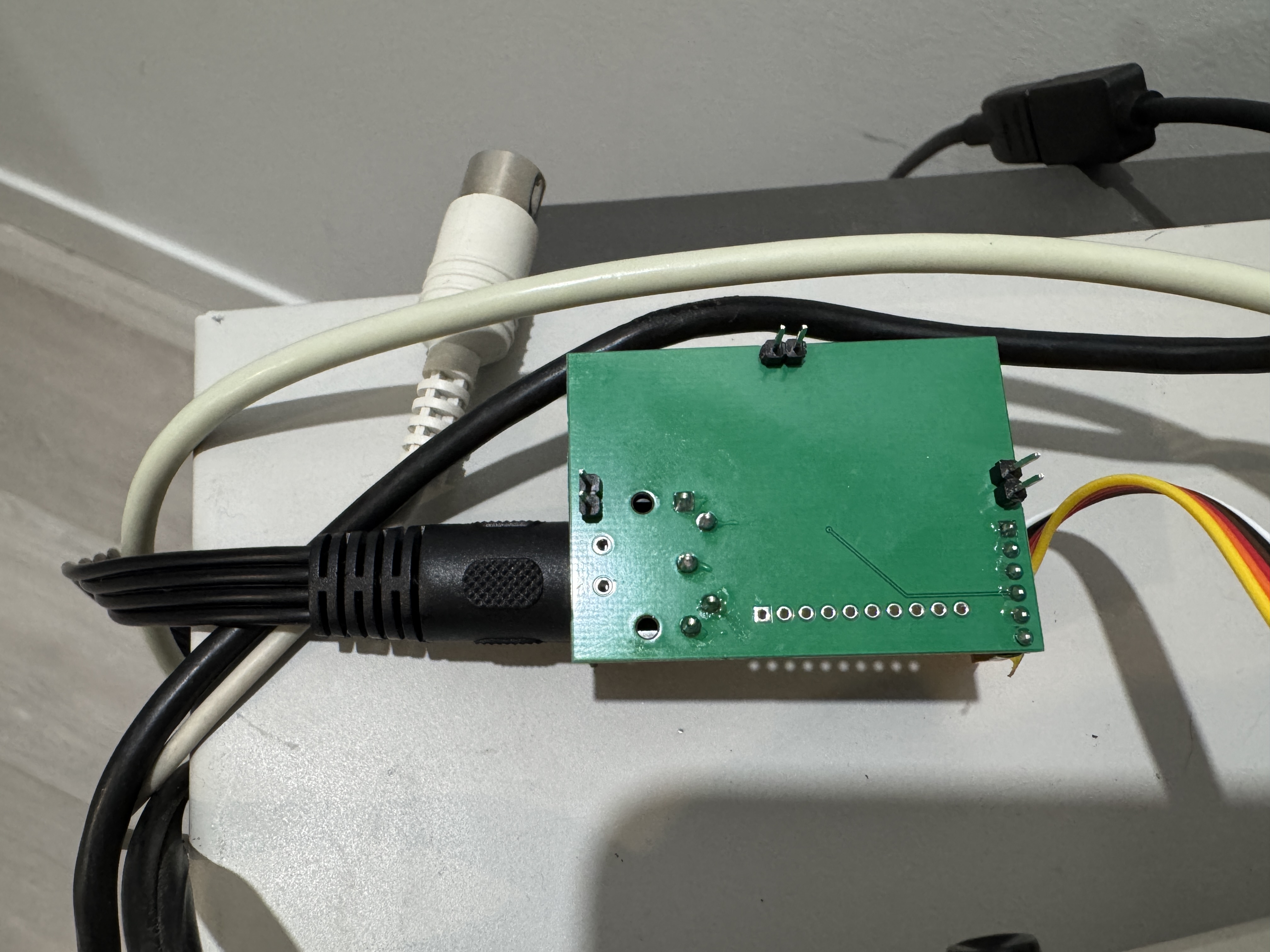 |
The completed installation brings the main board, ADDRMUX, PIA adapters, and AVIDEO board together:
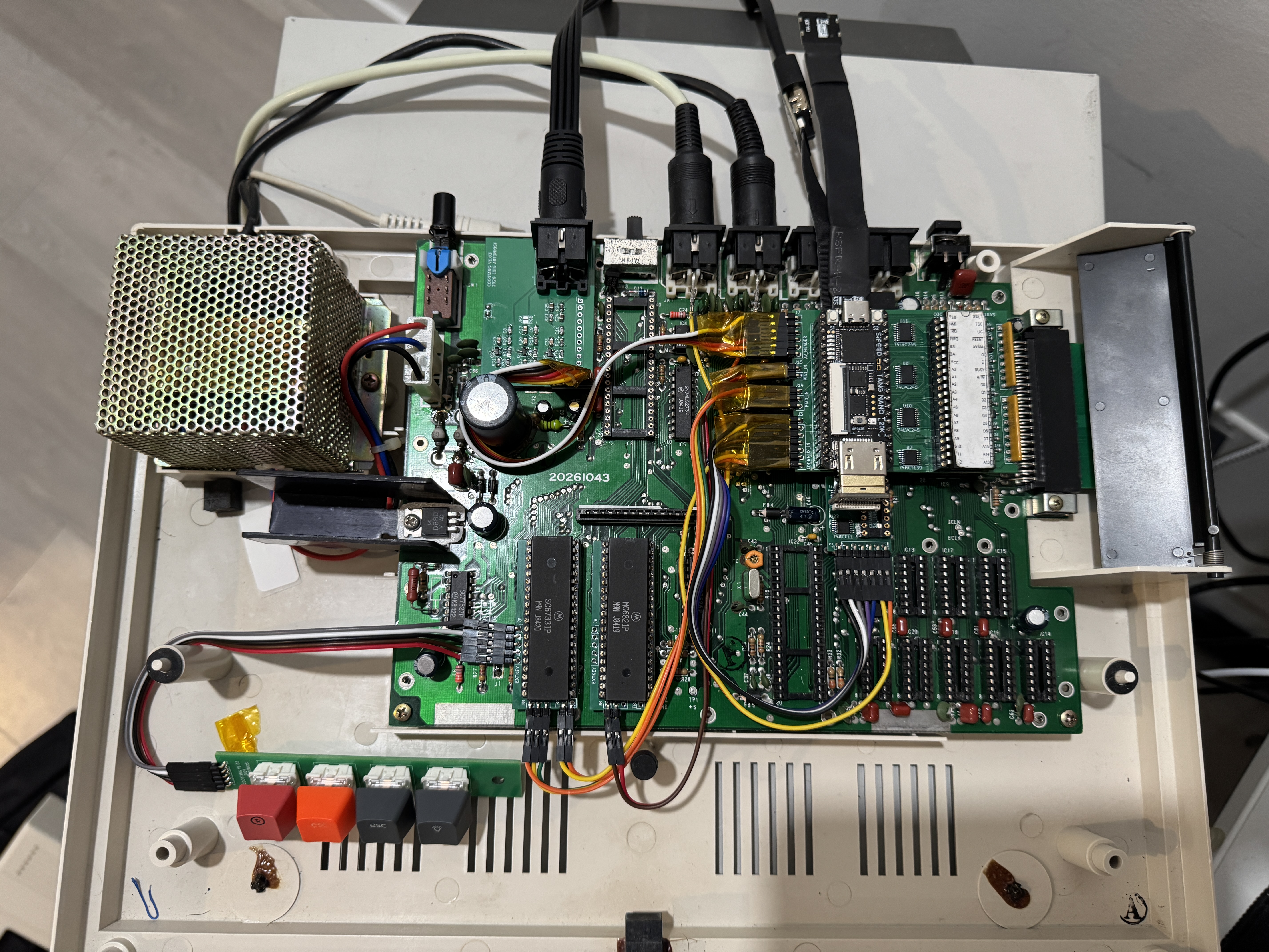
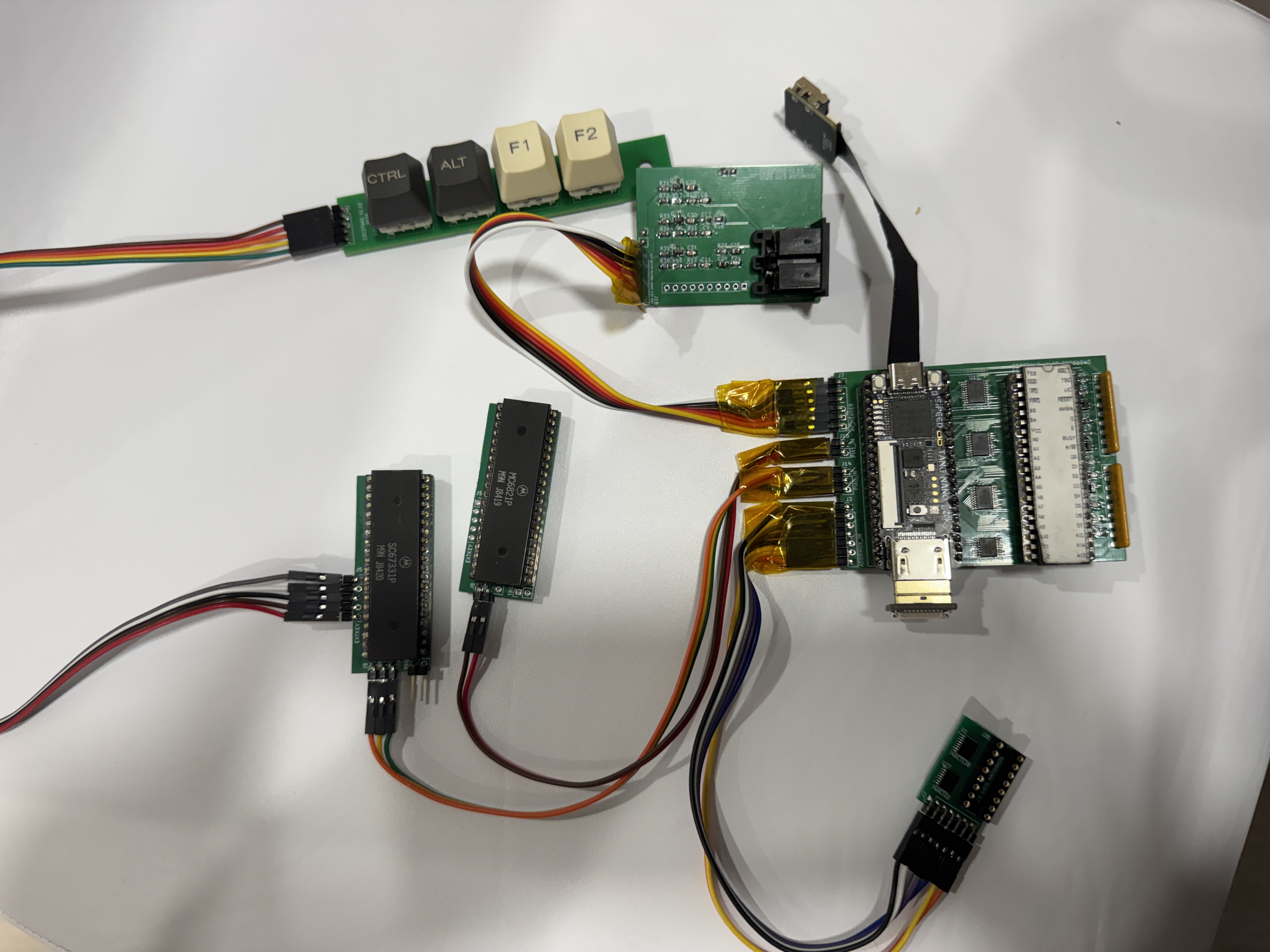
The photo below shows the fully assembled main board, PIA0, PIA1, ADDRMUX, AVIDEO, and external keyboard companion with their umbilical cables connected. Use it as an overview alongside the pin and bus map when connecting the boards.
With the original RF module removed, prepare its mounting position for AVIDEO. Remove the plastic spacers from the mounting header pins so the AVIDEO PCB can sit close to the motherboard. Leave the metal pins in place for soldering the board, as shown below.
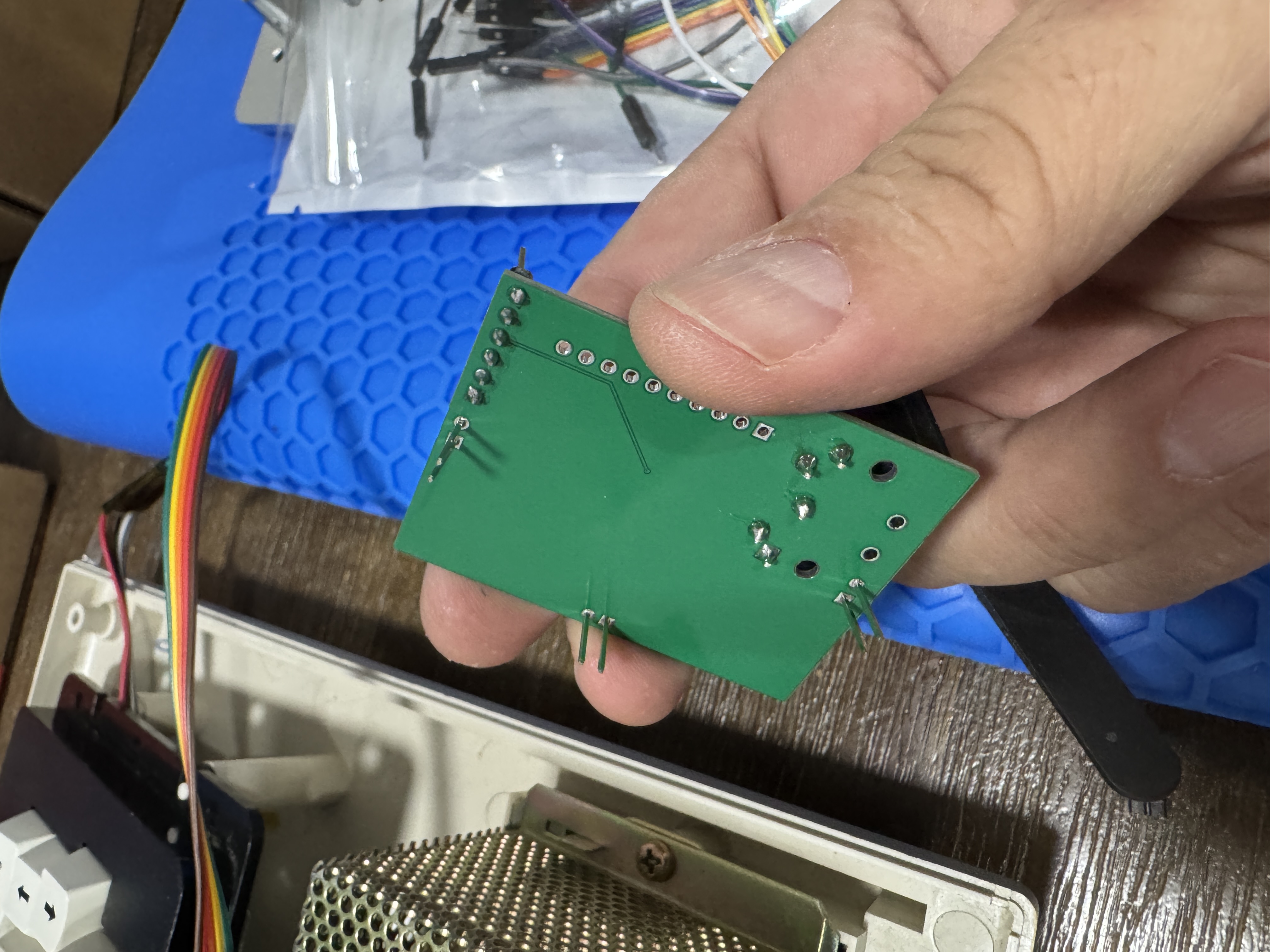
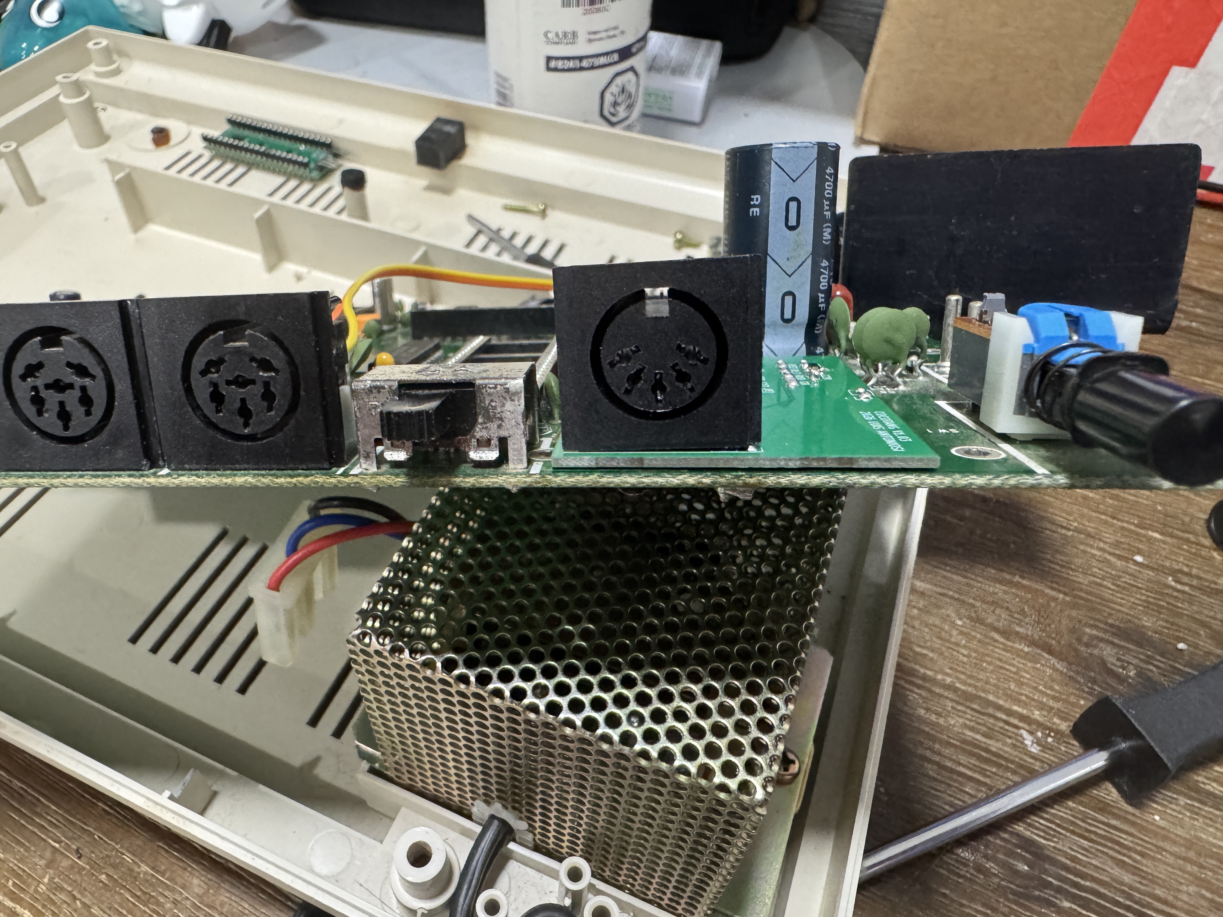
Clip all excess component leads and header-pin ends on the underside of AVIDEO, and remove excess solder that would prevent the board from sitting close to the motherboard. Retain the mounting pins needed to secure it. Fit the board over the prepared RF-area mounting pins, align the DIN-5 connector with the rear of the case, and solder the mounting pins with the PCB close to the motherboard. Keep clearance between the underside solder joints and the motherboard.
| Trimmed AVIDEO underside | Mounted board, side view |
|---|---|
 |  |
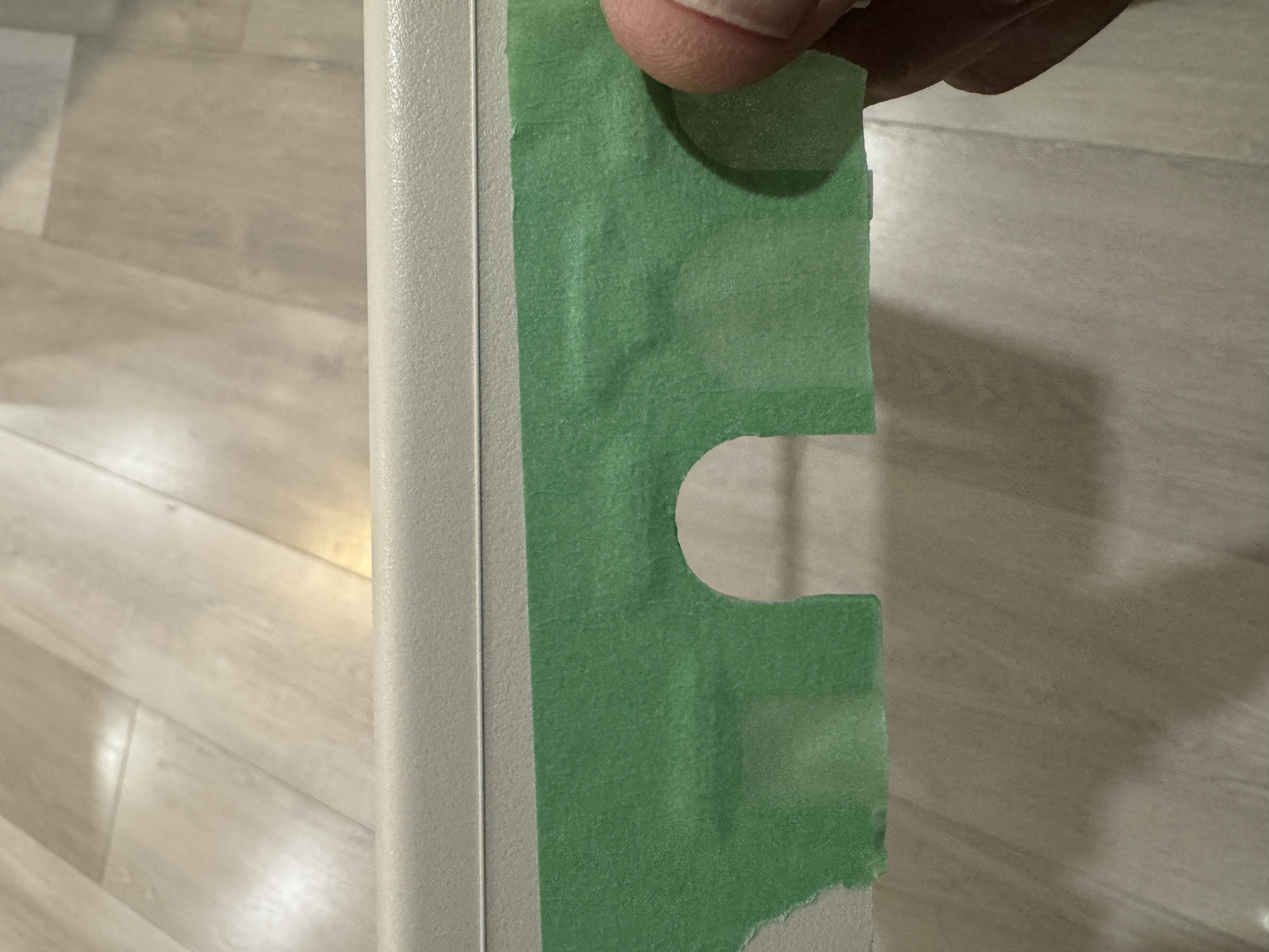
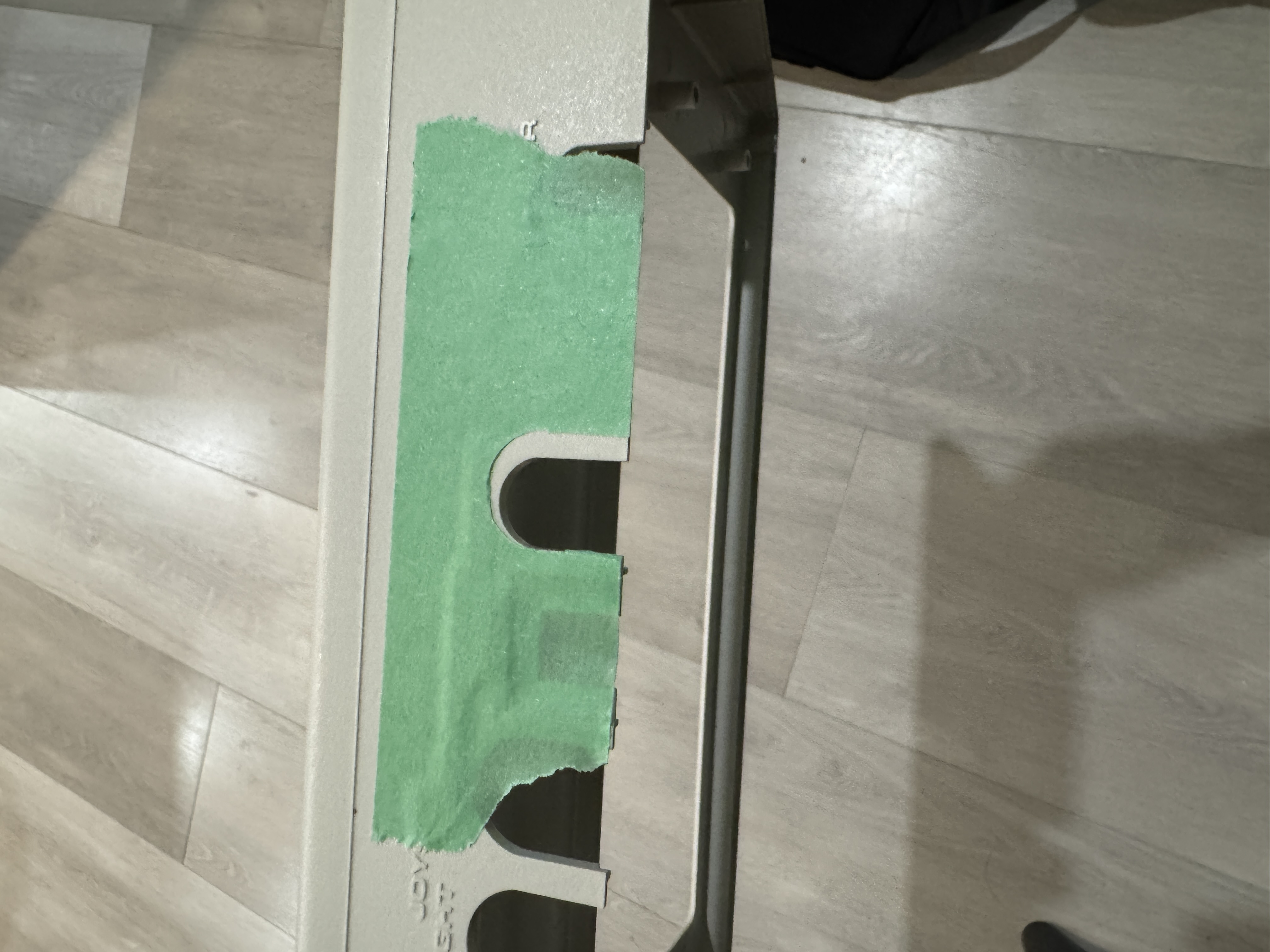
Use a neighboring DIN connector opening as a template. Apply masking tape over it and copy its outline by trimming the tape to match the opening. Peel off the tape and stick it over the original TO TV opening, aligning the bottom edge and checking its position against the installed AVIDEO connector. The transferred outline marks the enlarged opening needed for the DIN-5 plug.
| Copy the opening onto masking tape | Transfer the tape to the TO TV opening |
|---|---|
 |  |
Remove the cover from the computer before machining it. Use a Dremel or similar rotary tool with a bit like the one shown to enlarge the opening to the tape outline. Remove material gradually, smooth the edges, and check the fit of the DIN-5 plug. Clear away the plastic debris before refitting the cover.
| Rotary-tool bit | Finished opening |
|---|---|
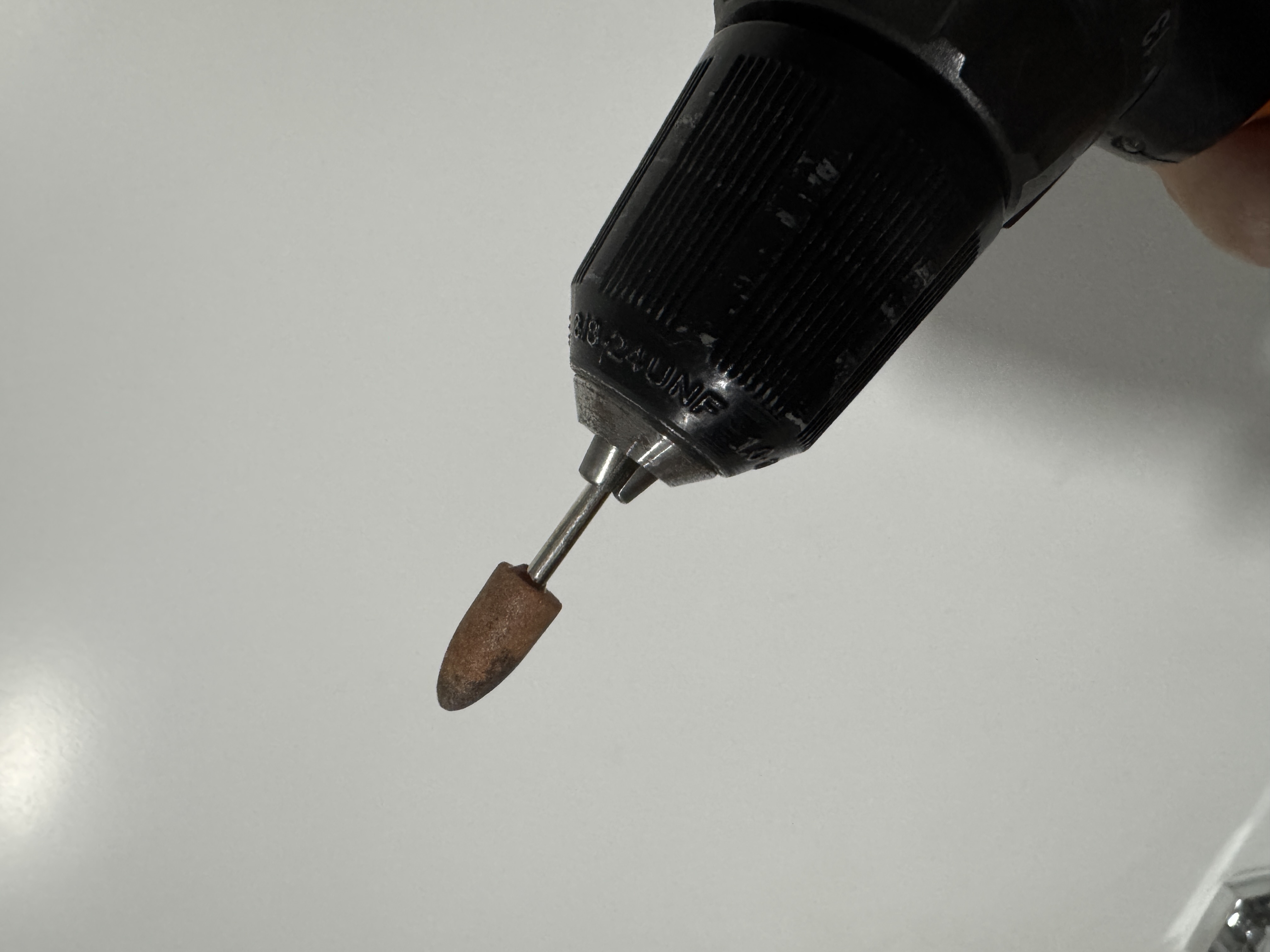 | 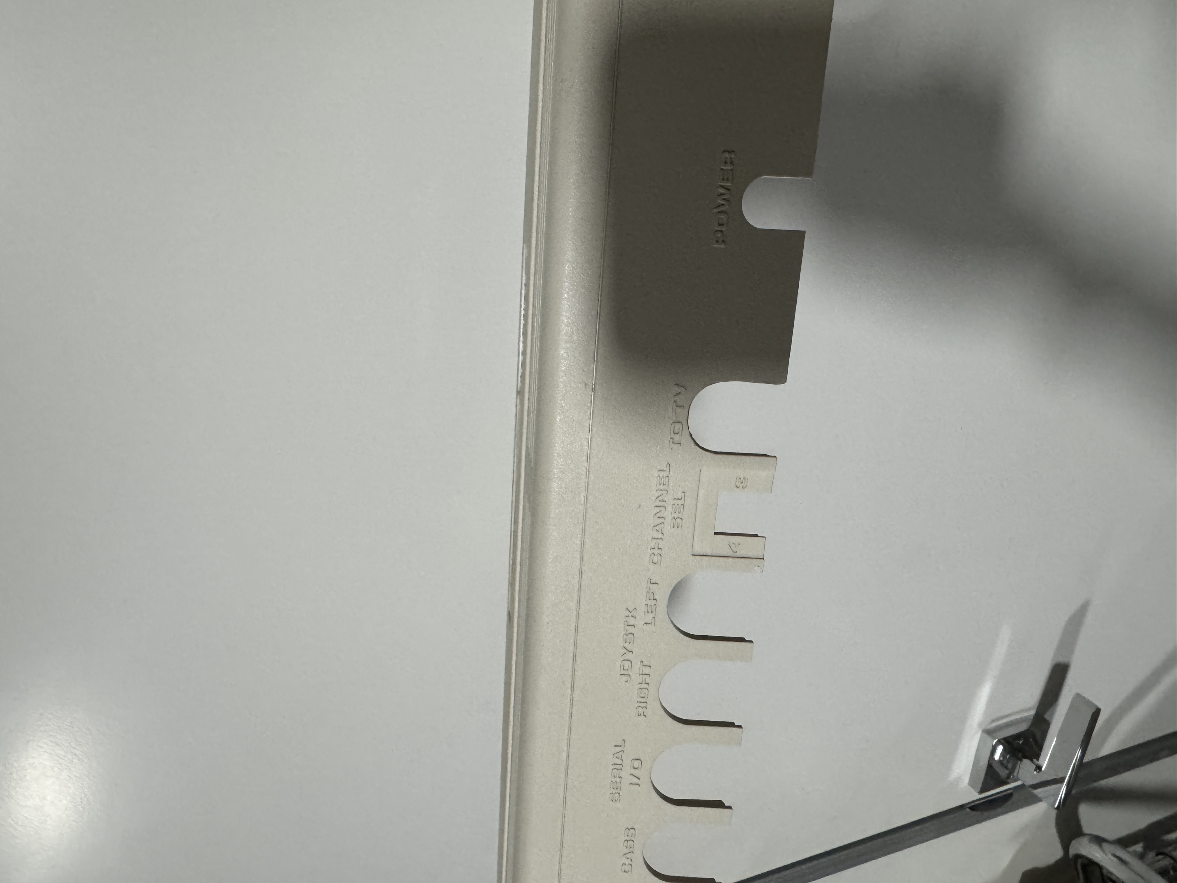 |
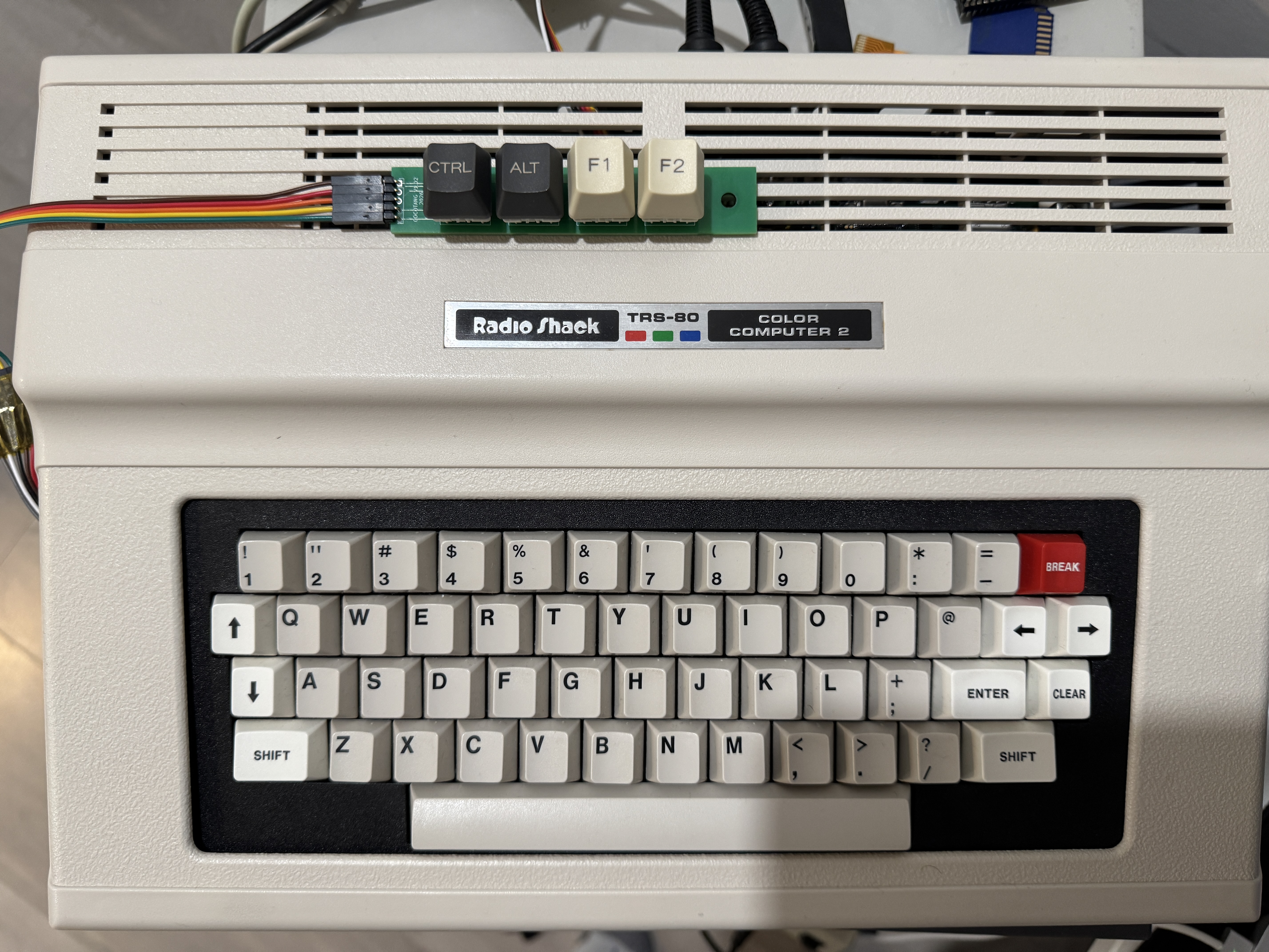
Refit the cover, checking that the internal cables are clear of its edges. The DIN-5 plug should fit through the enlarged opening and seat fully in the AVIDEO socket. The finished installation below shows the closed lid, connected DIN-5 cable, and external keyboard companion.
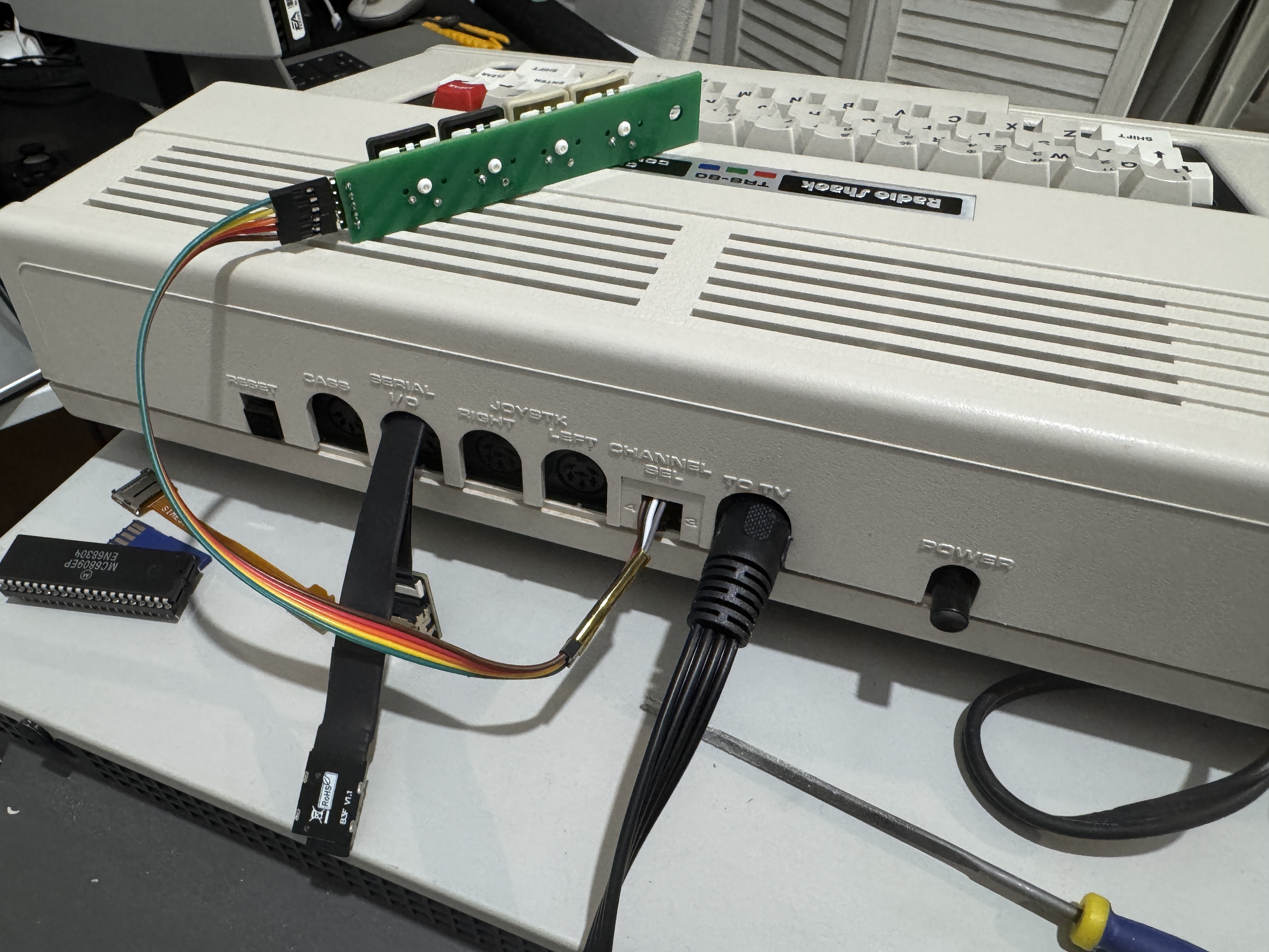
Both PIAs use the same adapter PCB, but they require different component populations and jumper settings:
The new PIA PCB also includes a pinout for an external keyboard. Populate and connect the external keyboard header only on PIA0.
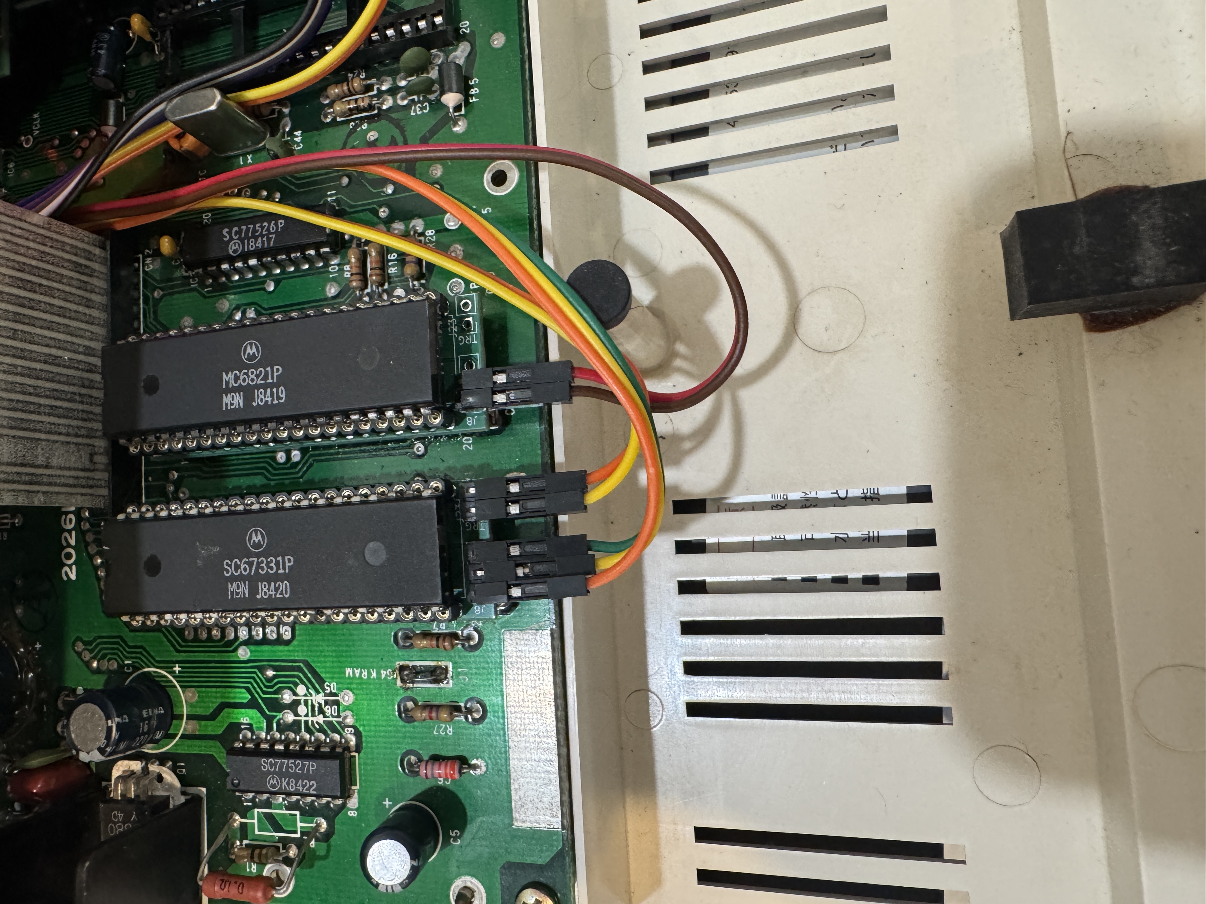
The optional four-key companion board uses 4 Cherry MX key switches, labeled CTRL, ALT, F1, and F2, and connects to the external keyboard header on PIA0. The photo shows the assembled companion beside the CoCo 2's built-in keyboard, with its cable attached. The PCB fabrication files are available as gerber_extkey.zip.
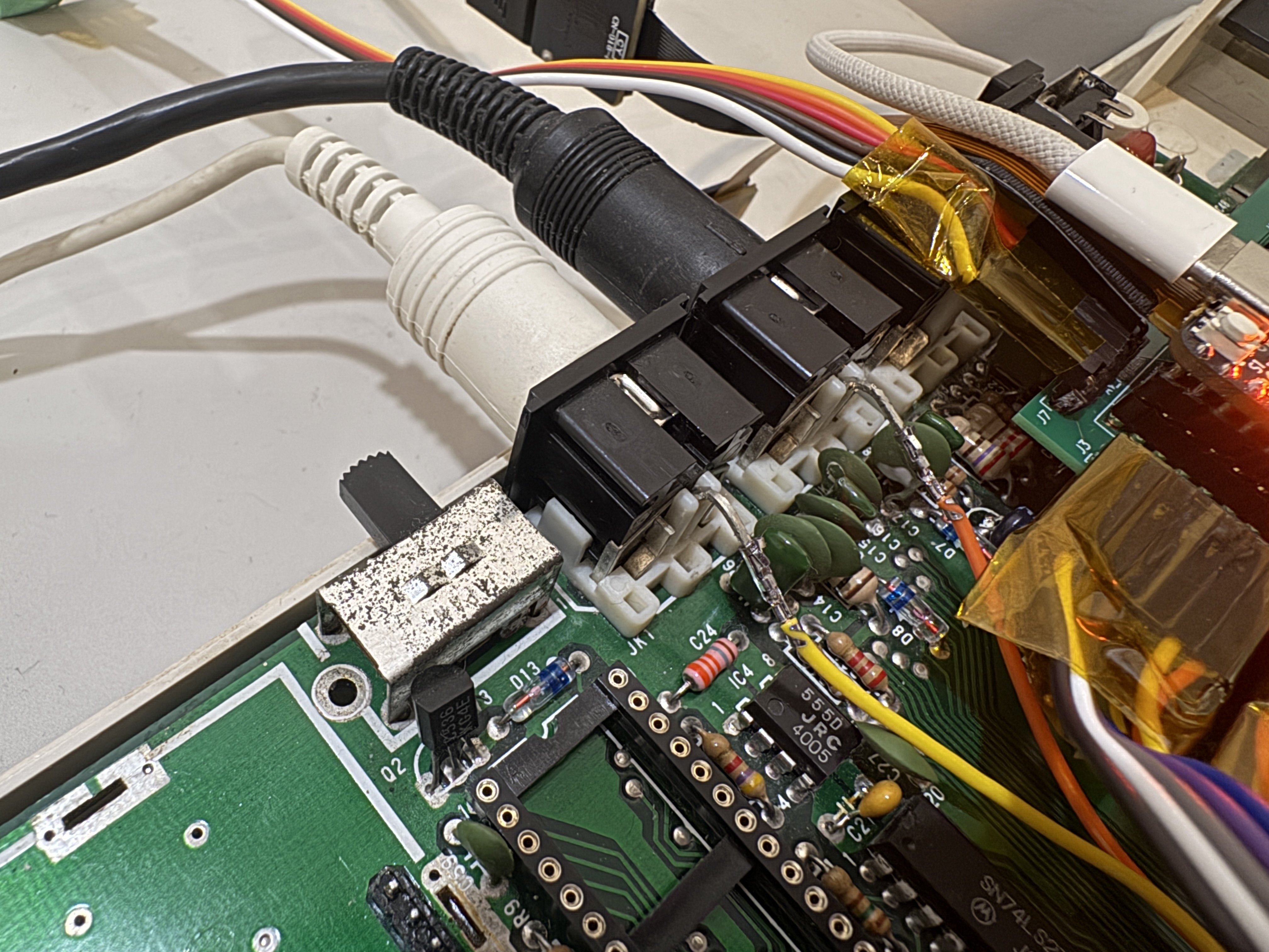
To support a second button on each joystick, disconnect pin 5 of each joystick connector from its original motherboard ground connection. Desolder the pin, pull it clear of the motherboard, and bend it upward as shown below. Keep the lifted pin clear of its original pad.
Use two jumper wires, one from each lifted pin, to connect the joystick second-button signals to the corresponding connections on the PIA0 adapter (SC67331P in the PIA photo above). To attach a jumper lead to a lifted pin, remove the plastic housing at that end and gently widen the metal contact to fit.
While the CPU is removed, you can replace the MC6809E with an HD6309E. NitrOS-9 supports the HD6309's native mode, and compatible applications can use its additional instructions. Choose the disk image that matches your installed CPU.
You can use this HDMI flat cable to expose the HDMI port outside the CoCo2 case. Being as flat just let it go through some port. Choose a model like A1-A4.
The optional CoCoTANG Audio/Video board provides a 5-pin DIN output and fits in the original RF modulator/shield location. Enlarge the cover opening for the connector and secure the PCB to the motherboard using the rear pin headers shown in the AVIDEO assembly photos. Follow the illustrated mounting and case-opening guide to prepare the RF area and enlarge the cover opening.
The revised J24 DIN-5 connector follows the Atari 800XL monitor pin assignment, with chroma connected to pin 5. The diagram shows the female socket viewed from the front, looking into the connector on the computer, with the keyway at the bottom. The cable plug's mating-face view is mirrored.
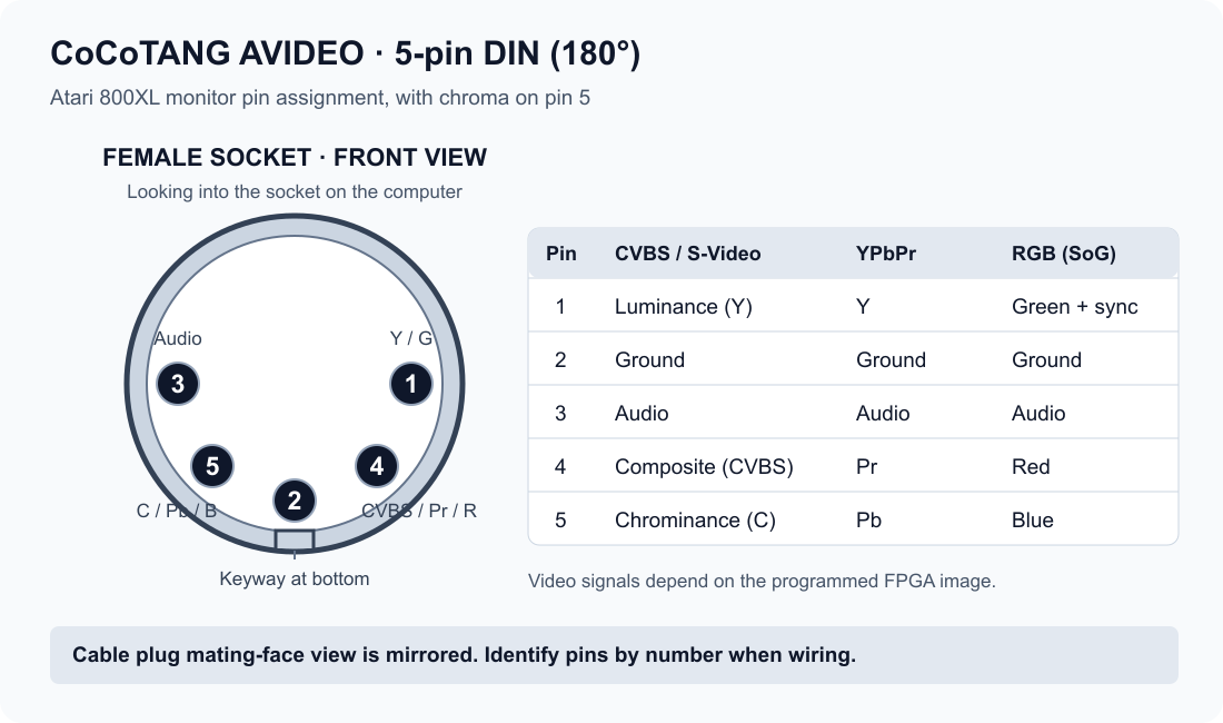
| DIN pin | CVBS / S-Video | YPbPr component | RGB with sync on green |
|---|---|---|---|
| 1 | Luminance (Y) | Y | Green + sync |
| 2 | Ground | Ground | Ground |
| 3 | Audio | Audio | Audio |
| 4 | Composite video (CVBS) | Pr | Red |
| 5 | Chrominance (C) | Pb | Blue |
Select the matching FPGA video image; the same physical pins carry different signals in each mode. For composite, use pins 4 (video), 3 (audio), and 2 (ground). For S-Video, use 1 (Y), 5 (C), and 2 (ground), with audio on pin 3.
For an example lead, see this 5-pin DIN to four-RCA cable; select the 5-pin version and verify its wiring against the table above.
Use an Atari 800XL-style monitor cable wired to this table for CVBS/S-Video. RGB and YPbPr need cables wired for their respective columns. Check the actual DIN pin connections rather than relying on RCA plug colors or the connector's pin count. This pinout applies to the revised AVIDEO PCB; check older boards before reusing a cable.
The assignments above match J24's current PCB nets: 1=G_Y, 2=GND, 3=AUDIO_RCA, 4=R_CVBS, 5=B_CHR. The diagram's editable source is din5-av-pinout.svg. For the Atari monitor-port reference, see the Atari 800XL service manual and Atari connector FAQ. CoCoTANG supplies chroma on pin 5, which was unconnected on many original 800XL machines.
YPbPr component: use a TV or monitor that accepts 15 kHz standard-definition 480i/240p signals over its component inputs, such as a compatible PVM or a CRT TV with YPbPr inputs. Check that the particular display accepts 240p; support for 480i alone does not guarantee it. Connect DIN pin 1 to Y, 5 to Pb, and 4 to Pr, with pin 3 for audio.
RGB with sync on green (SoG): use a cable wired specifically for CoCoTANG's RGB pinout and a display that accepts sync on green. On a compatible PVM, you can instead use the same 5-pin DIN to four-RCA lead linked above, with RCA-to-BNC adapters on the three video leads:
| DIN pin / lead | PVM input |
|---|---|
| 1 — Green + sync | G / Y |
| 4 — Red | R / Pr |
| 5 — Blue | B / Pb |
| 3 — Audio | Audio input |
Select RGB on the PVM and choose internal sync (INT), or turn EXT SYNC off, so it takes sync from green. The fourth RCA lead carries audio; a separate external-sync connection is not needed. For YPbPr, use the same three video connections but select component / YPbPr instead. Control names vary by model; see, for example, the Sony PVM-D14L5A/D20L5A operating instructions.
Download the appropriate CPU version of the CF disk image and write it to the microSD card used by CoCoTANG. These images require HDB-DOS, supplied by the optional cartridge or another supported ROM source.
On Linux, identify and unmount the card, then write the image to the whole device, replacing /dev/sdX with the correct device path:
sudo dd if=CF_6309.IMG of=/dev/sdX bs=1M
sync
The example uses the HD6309 image. Writing the image replaces the card's contents, so verify the destination device before running the command.
The standard build includes the Tandy Speech/Sound Cartridge (SSC) PSG and speech engine. SSC always starts disabled at cold boot. Press the CoCo motherboard RESET to advance through these selections:
| RESET presses since cold boot | Status label | SSC PSG and speech |
|---|---|---|
| 0 (cold boot) | ARTIFACT NORMAL | Disabled |
| 1 | ARTIFACT REVERSE | Disabled |
| 2 | NO ARTIFACT | Disabled |
| 3 | ARTIFACT NORMAL - SSC | Enabled |
| 4 | ARTIFACT REVERSE - SSC | Enabled |
| 5 | NO ARTIFACT - SSC | Enabled |
The next RESET returns to ARTIFACT NORMAL with SSC disabled. RESET is debounced, and holding it down advances only once. Disabled SSC stays silent, holds both synthesizers in reset, and leaves $FF7D/$FF7E available to the motherboard/cartridge bus. Software cannot enable SSC by writing its registers while an SSC-off selection is active.
HDMI shows the selected label for about four seconds. The analog banner is optional and off by default: set ENABLE_ANALOG_BANNER=1 in fpga/src/top_coco3.v and rebuild to include it. Its font is doubled in both dimensions, with each font row occupying two analog scanlines. This applies to RGB, YPbPr, CVBS, and S-Video; the HDMI label keeps its original size.
When SSC is selected, software resets its interface by writing 1 then 0 to $FF7D. $FF7E accepts commands/data and returns status; bit 7 high means ready. The implementation supports direct PSG register writes, buffered sound events/register streams, buffered AL2 allophones, and immediate ASCII text terminated by carriage return. English text uses NRL letter-to-sound rules; this is command-level compatibility rather than a TMS7040 CPU emulation. The speech interface source documents the supported commands.
PSG and speech are combined and mixed into both HDMI channels and the physical mono output at 1.5× gain (about +3.5 dB). The CoCo DAC and Orchestra-90 gains are unchanged. The final sum saturates at the signed PCM limits instead of wrapping, and disabling SSC clamps its contribution to silence.
In custom builds, ENABLE_SSC_SPEECH=0 removes speech while retaining the PSG; ENABLE_SSC_PSG=0 removes both SSC engines and restores the three artifact-only reset selections. make test-ssc-toggle checks the real top-level reset cycle, disabled bus/audio behavior, and both analog-banner settings using Gowin's installed simulation library.
Orchestra-90 audio is enabled by default and provides two 8-bit DACs without the cartridge ROM. Software writes unsigned samples to $FF7A (left) and $FF7B (right); 128 is the digital midpoint. Each channel holds its last sample until the next write. These are write-only DACs: reading the addresses does not change their values or provide readback.
Orchestra-90 requires no additional cartridge ROM or audio hardware. It is enabled by default in every normal machine image; no separate Orchestra-90 build is needed.
HDMI sends stereo PCM at 48 kHz. The existing CoCo PIA DAC is mixed equally into both channels at its normal gain; each Orchestra-90 DAC contributes at half gain, and the mixer clips at the signed PCM limits to prevent overflow. Both Orchestra-90 channels reset to the midpoint so they contribute silence before software uses them. The analog audio_out pin carries a mono mix of both Orchestra-90 channels and the CoCo PIA DAC. Each Orchestra-90 channel contributes at quarter gain to this downmix, while the CoCo PIA DAC keeps its normal gain; the sum is clipped before conversion to the physical 8-bit sigma-delta DAC.
To omit Orchestra-90 audio in a custom build, set the top_coco3 parameter ENABLE_ORCHESTRA90=0. Address and channel assignments follow XRoar's Orchestra-90 documentation and MAME's Orchestra-90 implementation.
Download GOWIN EDA Education for your OS from Gowin's official download page (an account may be required). Install the full EDA package, not only Gowin Programmer. The Education edition is intended for noncommercial education/research; check Gowin's current terms for your use.
Install openFPGALoader and, for simulation, Icarus Verilog (iverilog and vvp). On macOS, brew install openfpgaloader icarus-verilog is one option. On Debian/Ubuntu, sudo apt install openfpgaloader iverilog is one option. Linux may also need the openFPGALoader udev rules for non-root USB access.
From the FPGA directory, build and check the routed design:
cd fpga
make test
make rebuild
make timing
make test is optional for building the bitstream. Its current recipes write simulation executables to /private/tmp, so on Linux that directory must exist and be writable if you run the tests; make rebuild and make timing do not need it.
The output is fpga/impl/pnr/CoCoTANG.fs. make rebuild always runs synthesis and place-and-route; make build rebuilds only when Make considers an input newer than the bitstream. The Makefile expects Gowin at /Applications/GowinIDE.app/Contents/Resources/Gowin_EDA/IDE on macOS or /opt/Gowin/IDE on Linux. If yours is elsewhere, pass GOWIN_IDE=/path/to/Gowin_EDA/IDE to Make.
Each mode has its own bitstream and fixed video-mode setting, independent of the default ANALOG_VIDEO_MODE in src/top_coco3.v:
| Output | Build if needed and program | Program existing image | Bitstream in fpga/impl/pnr/ |
|---|---|---|---|
| RGB with sync on green | make program-rgb | make reprogram-rgb | CoCoTANG-rgb.fs |
| YPbPr component | make program-ypbpr | make reprogram-ypbpr | CoCoTANG-ypbpr.fs |
| NTSC CVBS and S-Video | make program-cvbs | make reprogram-cvbs | CoCoTANG-cvbs-minimal.fs |
Run these commands from fpga/. To build without programming, use make build-rgb, make build-ypbpr, or make build-cvbs. Use make rebuild-rgb, make rebuild-ypbpr, or make rebuild-cvbs to force a rebuild, and the corresponding make timing-rgb, make timing-ypbpr, or make timing-cvbs to check the routed timing. The reprogram-* targets never rebuild; their named image must already exist.
The artifact/SSC status banner is off on analog outputs by default. Set ENABLE_ANALOG_BANNER=1 in fpga/src/top_coco3.v and rebuild to enable its larger font in any analog video mode. The HDMI status label and reset selector are always available.
Run these commands from fpga/:
make build-all     # build missing or outdated images
make rebuild-all   # force synthesis and place-and-route for every image
Both targets cover six images: standard, RGB, YPbPr, CVBS/S-Video, PAL, and the standalone bus tester. The NTSC S-Video targets share the confirmed CVBS image, so it is built once. Logger/debug images are excluded.
Builds run sequentially, even with make -j, because Gowin shares the impl/ directory between projects. Every variant is attempted, and routed timing is checked after each successful build. The target returns a failure status if any build or timing check fails; it never programs the board or changes placement settings. Per-variant logs and summary.json are written to fpga/impl/build-all/ or fpga/impl/rebuild-all/.
The standalone bus tester is included in the aggregate builds. The normal production images keep the bus logger disabled; logger/debug projects are not restored by the aggregate targets.
For board bring-up, make data-test-program-sram builds the standalone bus tester if needed and loads it into FPGA SRAM for a temporary test. Use make data-test-program to store the tester in flash. It holds the CPU in reset and displays the data sweep and bus readback over HDMI. See the bus tester notes for controls and verification commands.
Connect the Tang Nano 20K by USB. The FPGA configuration and CoCo 3 ROM are two separate writes to the module's external SPI flash:
| Flash address | Contents | Command from fpga/ |
|---|---|---|
0x000000 | FPGA configuration (impl/pnr/CoCoTANG.fs) | make program or make reprogram |
0x100000 (1,048,576 decimal) | 32 KiB CoCo 3 ROM (roms/coco3.rom) | make rom |
cd fpga
make program     # builds if needed, then writes persistent FPGA configuration
make rom         # writes the ROM at 0x100000; needed for first setup
make reprogram flashes the existing bitstream without rebuilding. These Make targets use openFPGALoader's tangnano20k board support. The ROM offset is set by ROM_OFFSET=1048576 in the Makefile and by the FPGA flash loader; do not write the ROM at address zero, or it will overwrite the FPGA configuration. After both writes, power-cycle the board. The FPGA holds the CPU until its clocks, SDRAM, and ROM load are ready.
Run make data-test-program-sram from fpga/ to build the standalone bus tester if needed and load CoCoTANG-data-test.fs into the FPGA's volatile SRAM. The tester holds the CPU in reset and displays the data sweep, address bus readback, and control signals over HDMI. It does not need a CoCo 3 ROM.
This leaves the stored FPGA configuration and ROM unchanged. Power-cycling restores the configuration stored in flash.
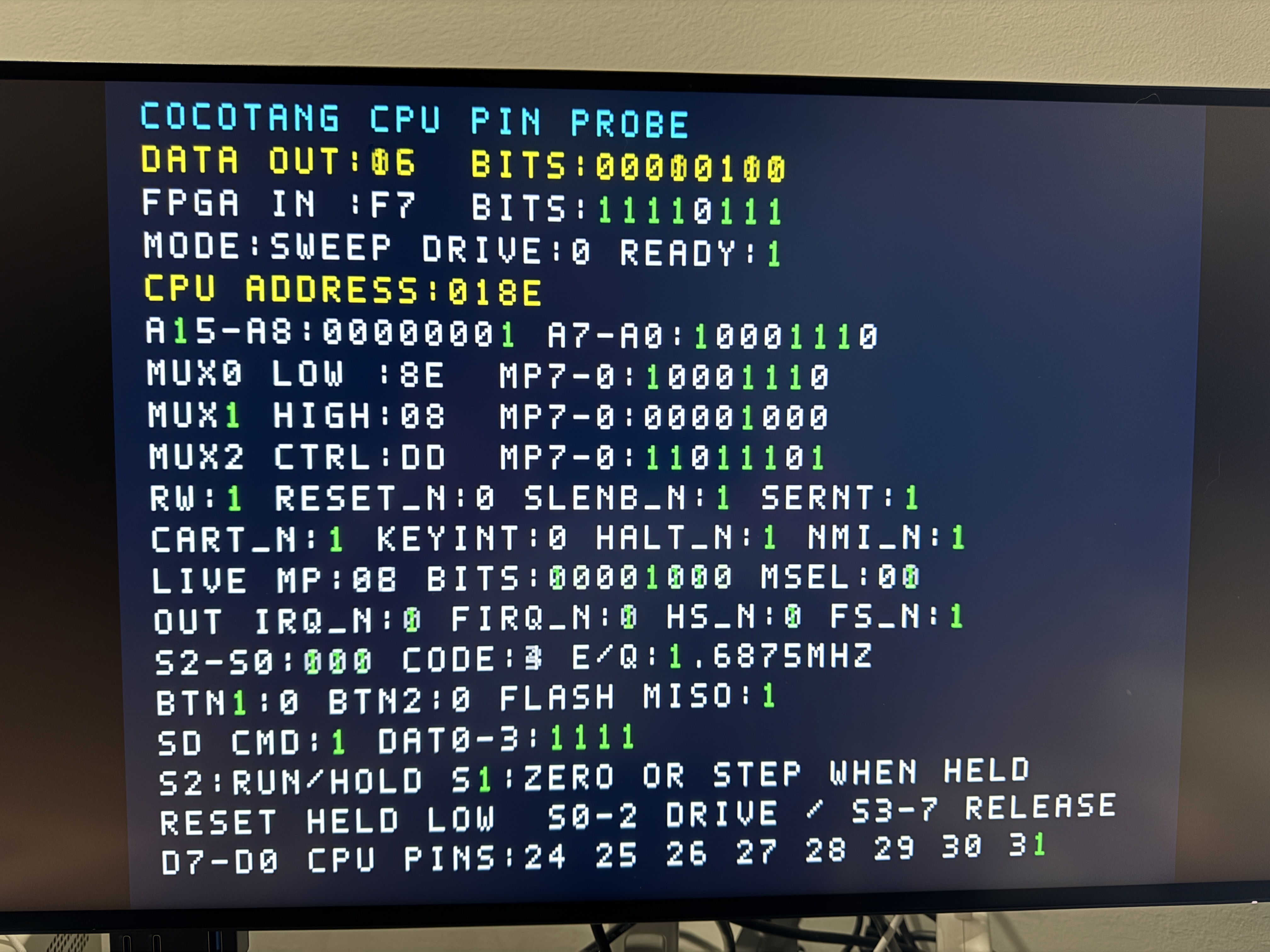
The tester helps locate missing connections, solder bridges, swapped bus lines, and faults in the bus buffers or address mux. FPGA IN shows the data bus at the FPGA side of the data transceiver. CPU ADDRESS and the A15–A8 / A7–A0 fields show the address sampled through the mux; the tester reads these lines rather than driving them.
Use the Tang Nano's S2 button to switch between sweep and hold. In hold mode, S1 advances the data byte and S code by one; in sweep mode, S1 restarts both at zero. The S code controls motherboard device selection, so hold mode is useful when probing a fixed condition.
Prepare for manual pin testing: turn off the computer and remove the CPU before attaching jumpers. Removing it lets you set each address line independently without fighting the CPU's outputs. Make connections on the CPU/motherboard side of the adapters, using motherboard ground and the board's normal logic levels; do not apply 5 V directly to Tang Nano pins.
Test each data line:
make data-test-program-sram and connect HDMI.RW:0 and DRIVE:0 before grounding any data pin. R/W low releases the FPGA's data outputs and selects the input direction through the data transceiver.FPGA IN goes low. The expected byte is $FE.$FD, $FB, $F7, $EF, $DF, $BF, and $7F. Remove each connection before testing the next pin. These values assume all ungrounded data lines remain high; floating inputs are not a reliable reference.DATA OUT is the sweep generator's requested byte. While DRIVE:0, it is not being driven onto the data bus, so it does not need to match FPGA IN. A pin that does not change its displayed bit suggests an open connection or buffer problem; a different bit changing suggests swapped wiring, and two bits changing together suggests a short.
Test each address line:
CPU ADDRESS and the address bit fields. With all other address lines high, grounding A0 gives $FFFE, grounding A1 gives $FFFD, and grounding A15 gives $7FFF.MUX0 LOW for A0–A7 and MUX1 HIGH for A8–A15. The high-address mux uses a remapped bit order; use the decoded address fields to identify CPU address bits.A line that never changes can indicate an open joint, missing connection, or buffer/mux fault. An unexpected address bit changing can indicate incorrect wiring or an address-remap problem. The display shows the FPGA's sampled result; a meter or logic analyzer at the CPU socket and buffer pins helps locate where the signal is lost.
Turn off the computer before removing the test jumpers or reinstalling the CPU. Remove the R/W ground connection before returning to normal operation. Power-cycling also restores the FPGA image stored in flash.
For Windows, use the Gowin Programmer supplied with Gowin EDA Education (or Gowin's standalone Programmer). The repository's Makefile is written for macOS/Linux and uses openFPGALoader; it is not a native Windows programming recipe. Gowin's Programmer User Guide describes the device-configuration dialog.
fpga/impl/pnr/CoCoTANG.fs.fpga/impl/pnr/CoCoTANG.fs, set External Flash Options → Start Address to 0x000000, save, then click Program/Configure.fpga/roms/coco3.rom under FW/MCU/Binary Input Options → Firmware/Binary File, choose Generic Flash if a flash-device choice is required, and set External Flash Options → Start Address to 0x100000. Save and program. The dialog wording varies between Gowin releases; the important distinction is the raw-binary operation and the 1 MiB start address.Windows USB driver choice: Gowin Programmer and openFPGALoader may require different USB drivers. The normal Windows path above uses Gowin's driver. If you choose to use openFPGALoader on Windows instead, install its Windows build and use Zadig to bind WinUSB to the Tang Nano 20K's programming/JTAG interface (enable Options → List All Devices if necessary). Check the device/interface identity before clicking Install/Replace Driver—do not replace an unrelated USB interface. Switching to WinUSB can stop Gowin Programmer from seeing the board; restore the Gowin driver in Device Manager or reinstall it when returning to Gowin Programmer. libusb's Windows guidance recommends WinUSB for libusb applications.
This is an actively developed hardware/RTL project. Review the pin and bus map, fabrication drawing, and KiCad files before building hardware. Flashing a new FPGA image or ROM changes the board's nonvolatile contents; keep a known-good image available while experimenting.
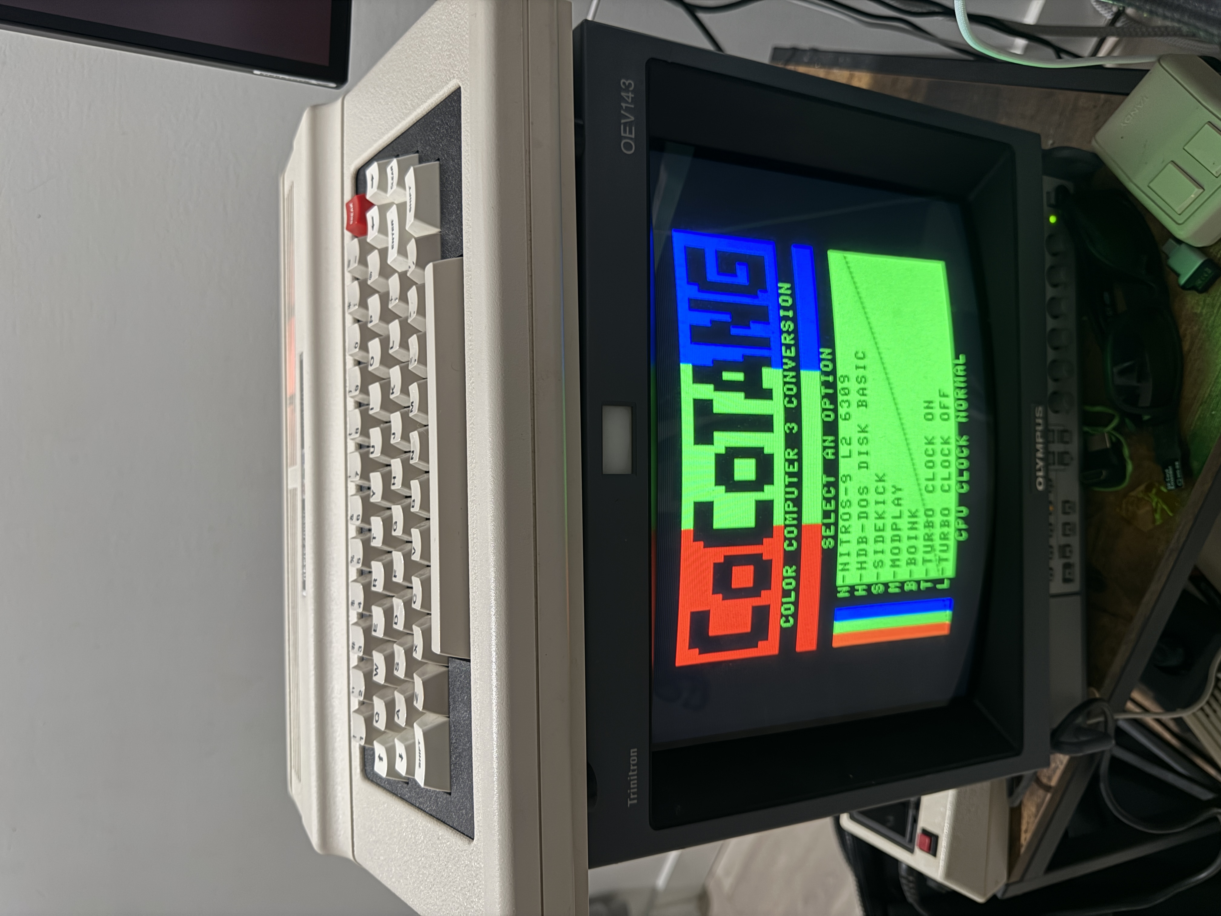
Games, NitrOS-9, and a graphics demo running on CoCoTANG:
| Calixto Island | Contras |
|---|---|
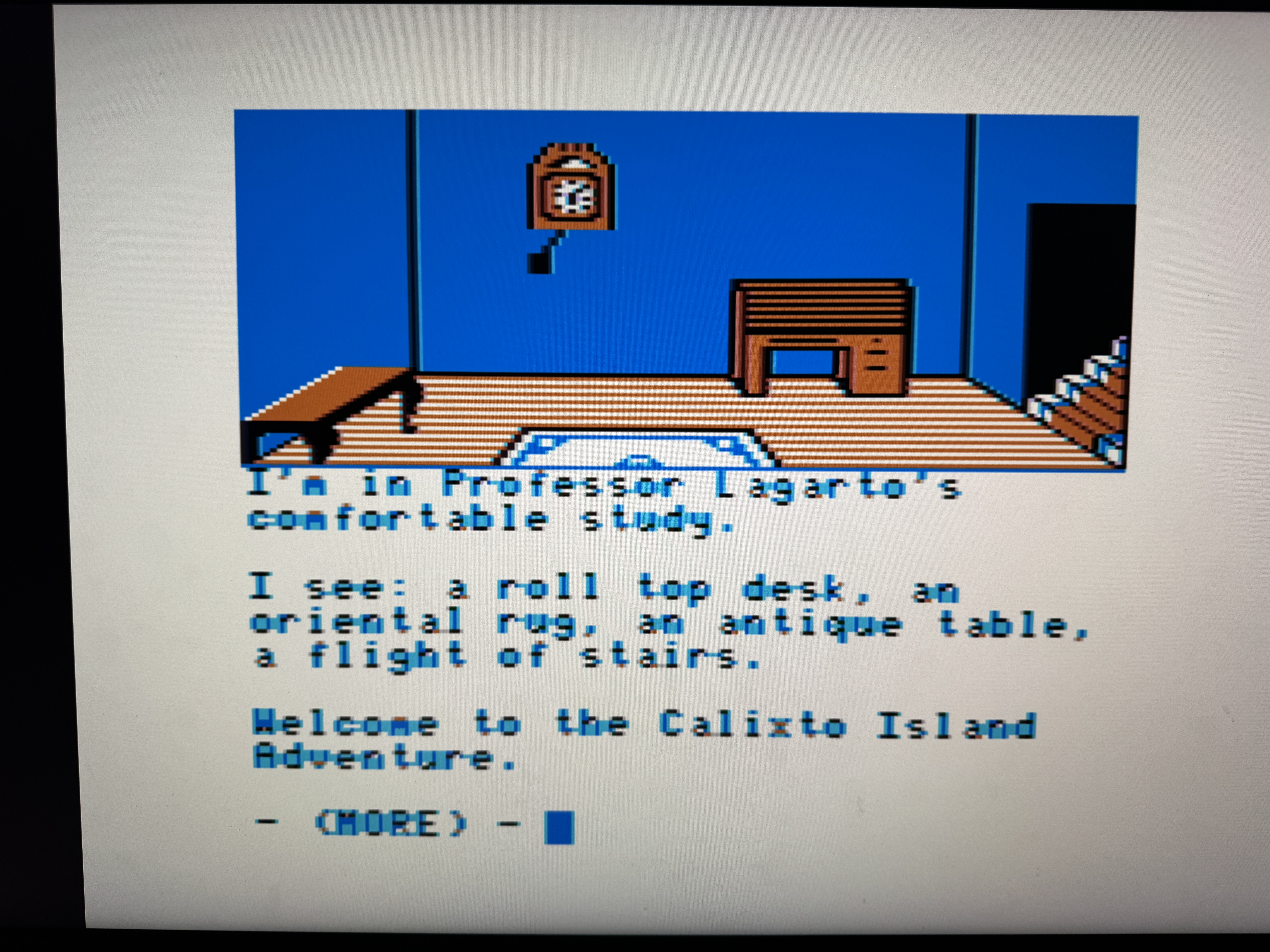 | 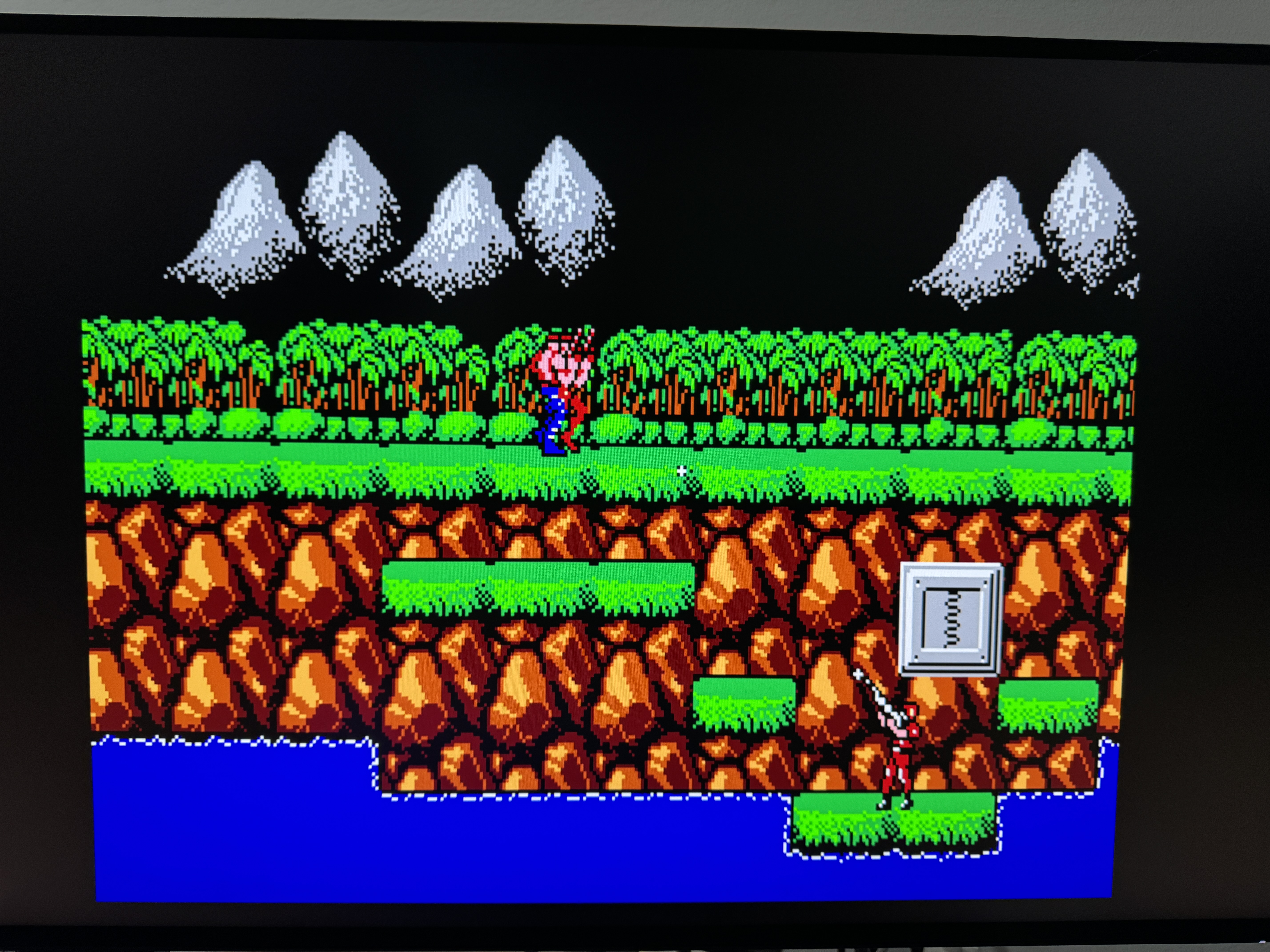 |
| NitrOS-9 | Sock Master's Drive Thru demo |
|---|---|
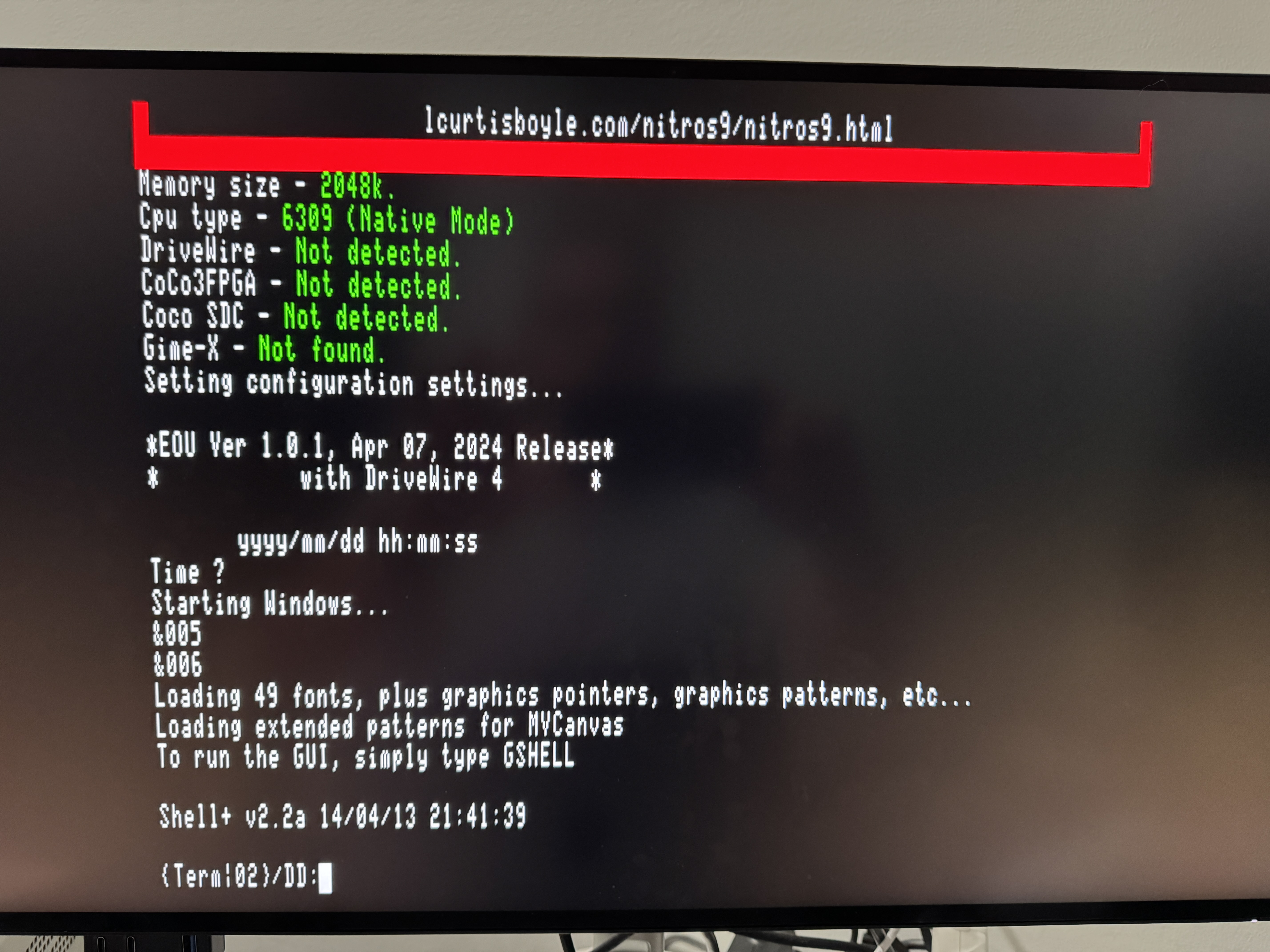 | 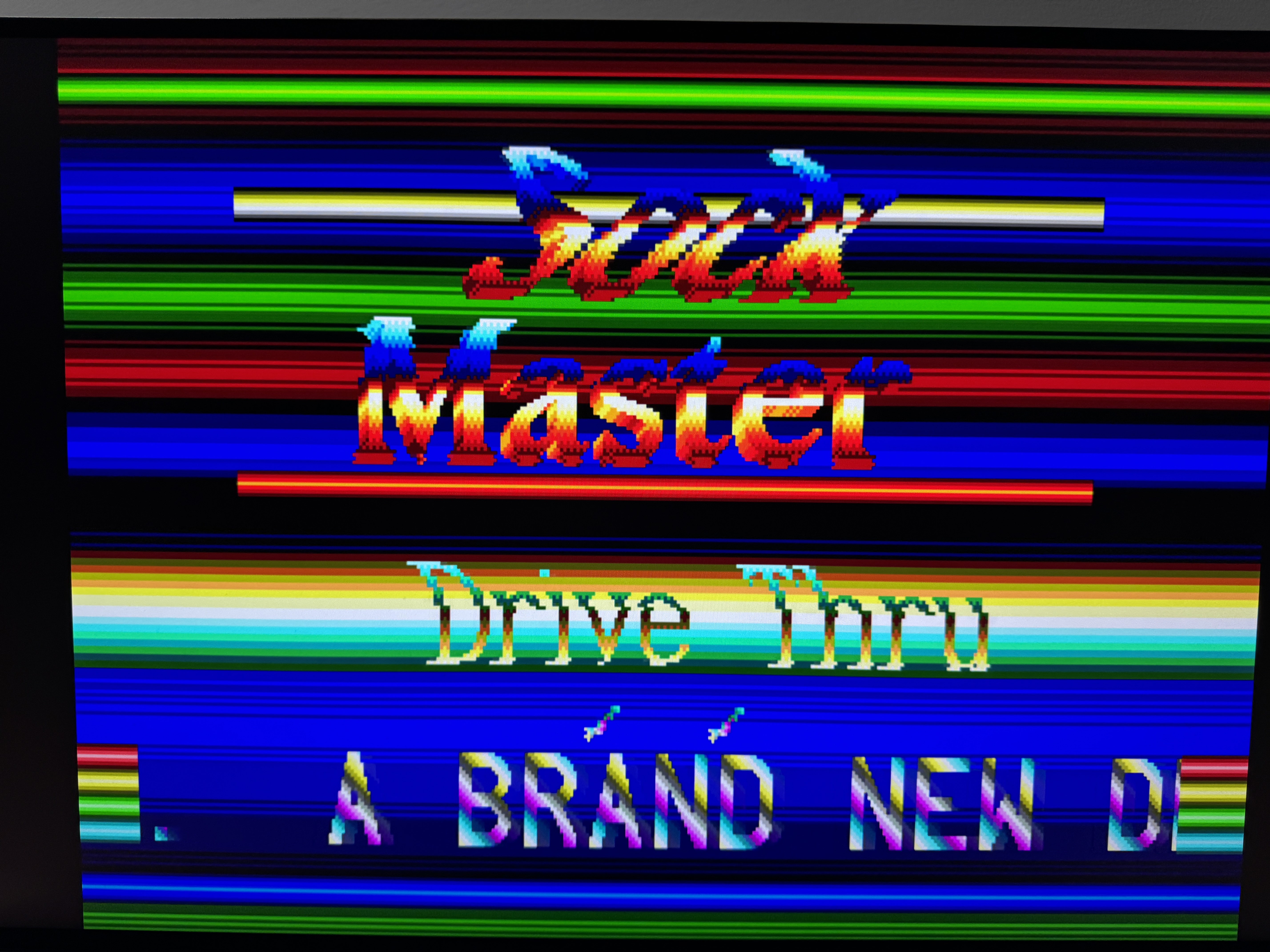 |
| Qty | Value | Footprint | References |
|---|---|---|---|
| 19 | 104 | Capacitor_SMD:C_0805_2012Metric_Pad1.18x1.45mm_HandSolder | C1, C2, C3, C4, C13, C14, C15, C16, C18, C19, C29, C30, C31, C32, C33, C34 +3 |
| 11 | 4.7K | Resistor_SMD:R_0805_2012Metric_Pad1.20x1.40mm_HandSolder | R3, R5, R7, R13, R19, R20, R21, R22, R32, R34, R36 |
| 9 | MMBT3904-TP | FPGA_Common:SOT-23_MCC | Q1, Q2, Q3, Q4, Q5, Q6, Q7, Q8, Q9 |
| 8 | 74LVC245 | Package_SO:TSSOP-20_4.4x6.5mm_P0.65mm | U4, U8, U10, U11, U12, U13, U14, U15 |
| 7 | 1K | Resistor_SMD:R_0805_2012Metric_Pad1.20x1.40mm_HandSolder | R1, R16, R17, R23, R31, R33, R35 |
| 6 | 10K | Resistor_SMD:R_0805_2012Metric_Pad1.20x1.40mm_HandSolder | R2, R4, R6, R14, R15, R18 |
| 4 | 4.7K | Resistor_THT:R_Array_SIP9 | RN1, RN2, RN3, RN4 |
| 4 | 47K | Resistor_SMD:R_0805_2012Metric_Pad1.20x1.40mm_HandSolder | R8, R9, R25, R26 |
| 3 | 470pF | Capacitor_SMD:C_0805_2012Metric_Pad1.18x1.45mm_HandSolder | C8, C9, C11 |
| 3 | 75 | Resistor_SMD:R_0805_2012Metric_Pad1.20x1.40mm_HandSolder | R10, R11, R12 |
| 3 | SUPPORT | Connector_PinSocket_2.54mm:PinSocket_1x02_P2.54mm_Vertical | J11, J20, J22 |
| 2 | 1800pF | Capacitor_SMD:C_0805_2012Metric_Pad1.18x1.45mm_HandSolder | C10, C12 |
| 2 | 74HC139 | Package_SO:TSSOP-16_4.4x5mm_P0.65mm | U3, U6 |
| 2 | 74HCT245 | Package_SO:TSSOP-20_4.4x6.5mm_P0.65mm | U9, U16 |
| 2 | ADDRMUX_IN | Connector_PinHeader_2.54mm:PinHeader_1x07_P2.54mm_Vertical | J3, J17 |
| 2 | AV_HEADER | Connector_PinSocket_2.54mm:PinSocket_1x06_P2.54mm_Vertical | J7, J10 |
| 2 | CPU | FPGA_Common:DIP-40_W15.24mm-OVERSIZED | J1, J19 |
| 2 | PIA0_IN | Connector_PinHeader_2.54mm:PinHeader_1x03_P2.54mm_Vertical | J14, J16 |
| 2 | PIA1_IN | Connector_PinHeader_2.54mm:PinHeader_1x02_P2.54mm_Vertical | J12, J15 |
| 2 | SD103BW | Diode_SMD:D_SOD-123F | D1, D3 |
| 2 | SS14 | Diode_SMD:D_SMA | D2, D4 |
| 2 | Tang_Nano_20k | FPGA_Common:Tang_Nano_20k | U5, U17 |
| 1 | 100K | Resistor_SMD:R_0805_2012Metric_Pad1.20x1.40mm_HandSolder | R24 |
| 1 | 1uF | Capacitor_SMD:C_0805_2012Metric_Pad1.18x1.45mm_HandSolder | C17 |
| 1 | 4.7uF | Capacitor_SMD:C_0805_2012Metric_Pad1.18x1.45mm_HandSolder | C25 |
| 1 | 6.8nF | Capacitor_SMD:C_0805_2012Metric_Pad1.18x1.45mm_HandSolder | C24 |
| 1 | 74HCT11 | Package_SO:TSSOP-14_4.4x5mm_P0.65mm | U22 |
| 1 | 74HCT138 | Package_SO:TSSOP-16_4.4x5mm_P0.65mm | U1 |
| 1 | 74HCT30 | Package_SO:TSSOP-14_4.4x5mm_P0.65mm | U7 |
| 1 | ADDRMUX | FPGA_Common:DIP-16_W7.62mm-OVERSIZED | J28 |
| 1 | ADDRMUX_OUT | Connector_PinHeader_2.54mm:PinHeader_1x07_P2.54mm_Vertical | J2 |
| 1 | ALT | Button_Switch_Keyboard:SW_Cherry_MX_1.00u_PCB | SW1 |
| 1 | AT28C64B-15PU | FPGA_Common:28P6_ATM | U2 |
| 1 | AUTOSTART | Jumper:SolderJumper-2_P1.3mm_Open_Pad1.0x1.5mm | JP1 |
| 1 | AV | FPGA_Common:SWITCHCRAFT_57PC5F | J24 |
| 1 | CMP_IN | Connector_PinHeader_2.54mm:PinHeader_1x06_P2.54mm_Vertical | J18 |
| 1 | CTRL | Button_Switch_Keyboard:SW_Cherry_MX_1.00u_PCB | SW2 |
| 1 | CoCo_Cart | FPGA_Common:COCO_CART | J13 |
| 1 | EXTKEY | Connector_PinSocket_2.54mm:PinSocket_1x05_P2.54mm_Vertical | J5 |
| 1 | EXTKEY_IN | Connector_PinSocket_2.54mm:PinSocket_1x05_P2.54mm_Vertical | J9 |
| 1 | F1 | Button_Switch_Keyboard:SW_Cherry_MX_1.00u_PCB | SW3 |
| 1 | F2 | Button_Switch_Keyboard:SW_Cherry_MX_1.00u_PCB | SW4 |
| 1 | MountingHole | MountingHole:MountingHole_4.3mm_M4 | H1 |
| 1 | PIA0 | Jumper:SolderJumper-2_P1.3mm_Open_Pad1.0x1.5mm | JP3 |
| 1 | PIA0 | FPGA_Common:DIP-40_W15.24mm-OVERSIZED | J4 |
| 1 | PIA0_OUT | Connector_PinHeader_2.54mm:PinHeader_1x03_P2.54mm_Vertical | J8 |
| 1 | PIA1 | Jumper:SolderJumper-2_P1.3mm_Open_Pad1.0x1.5mm | JP4 |
| 1 | RGB_CVBS | Connector_PinSocket_2.54mm:PinSocket_1x03_P2.54mm_Vertical | J21 |
| 1 | SUPPORT | Connector_PinHeader_2.54mm:PinHeader_1x10_P2.54mm_Vertical | J6 |
| 1 | TRG | Connector_PinHeader_2.54mm:PinHeader_1x02_P2.54mm_Vertical | J23 |
It measures 236.8 × 129.1 mm and has 2 copper layers, 1.6 mm thick.
127 parts, built around the 74LVC245AD, 74HCT245, 74HC139D and 74HCT11D. The full list of its parts is on this page, with links to each part's symbol and footprint where PCBKit's library has them.
From the lfantoniosi/CoCoTANG repository on GitHub, at the commit this page was made from: the board is kicad/CoCoTANG.kicad_pcb and its schematic kicad/CoCoTANG.kicad_sch. PCBKit opens the board in the browser, with nothing to install.
Its repository states no licence, so its author keeps all rights: ask lfantoniosi before reusing the design.

ksr/p8x
Generated by generators/genkicad.py from the canonical geneagle netlist (CARDS["peripheral-card"]), same standard as the memory card: 4-layer (F/B signals, In1=GND, In2=VCC planes), a bypass cap above each IC, a…


mgoegel/robotron-esp-vga.pcb
Robotron MDA Adapter, ESP32S3 based PCB Layout in KiCad 8.0

PUT-Motorsport/PUTM_EV_IMD_SAFETY
Bender Insulation Monitoring Device Shutdown Circuit driver, based on TW & SS project