2 layers258.1 × 122.9 mm
FrontPanel
89Mods/LVDC
Replica of the Launch Vehicle Digital Computer using 74-series logic
124 parts2MIT
 89Mods/LVDC2
Replica of the Launch Vehicle Digital Computer using 74-series logic
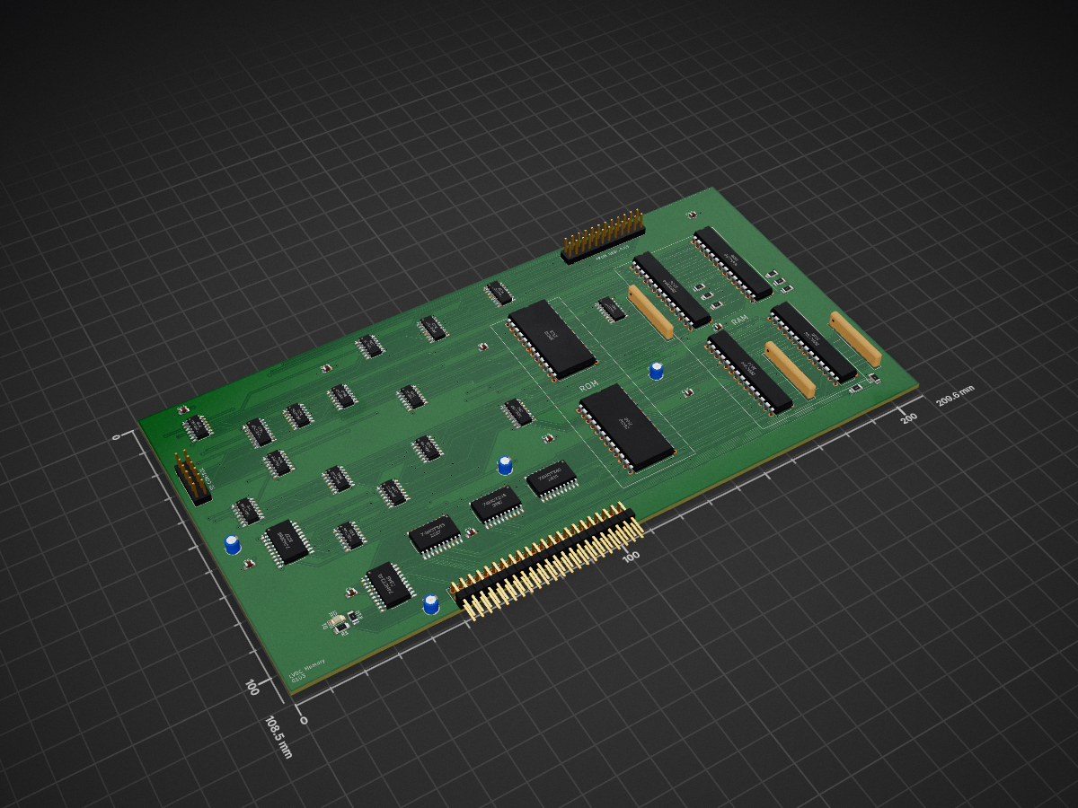
Memory is an open-source printed circuit board by 89Mods, from the 89Mods/LVDC repository on GitHub, published under the MIT licence. It is a 4-layer board of 209.5 × 108.5 mm with 58 parts on 174 nets, routed with 2,478 tracks and 297 vias.
It is built around the 74HCT245, 74HCT157D and 74HCT08D, with the 74HCT11D, 74HCT32D and 74HC02 among its other parts. Its parts include 27 ICs, 14 capacitors, 10 resistors, 3 connectors and 1 diode.


Replica of the Launch Vehicle Digital Computer using 74-series logic. This projects only aims to keep the CPU Architecture binary-compatible with the original. Implementation details, IO Peripherals and Software are all originally created by me. This is party due to the fact that detailed hardware descriptions (i.e. schematics) are not as abundant for the LVDC as for the AGC, but also because this project doubled as a challenge to myself to implement such an odd instruction set, but using every trick I’ve learned from my years of engineering integrated circuit layouts. It turns out that applying nanoscale engineering tricks to a macroscale discrete logic build can work out quite well. The clock speed of this computer is 2.5MHz, but it can probably go faster.
This LVDC is accurate to the original in the sense that it executes the same instructions that function the exact same, has the same memory layout (including special locations like HOP save and MQ) and can execute snippets of original LVDC code.
The differences are:
Infact, I took the most liberties with the IO Card, which contains various modern components hooked into the CPU’s IO Bus. Its mostly a random mashup of things I thought would be cool (there is even a Commodore SID replica in there) to demonstrate the computer with.
The most significant addition is that of a front panel (the original LVDC was an embedded device with no user interface) which is a bit like a DSKY, but stripped down and only capable of displaying in hexadecimal. The panel is optional. I can be safely removed and the computer used as a true embedded device.
Software wise, things are still WiP. Two ROMs provide just enough storage for a small bootloader to initialize the entire SRAM from a flash IC. Sadly, core memory is far too bulky and expensive, so this will have to do. I created a mini-OS for this system that allows a user to control the computer by typing in commands consisting of a Noun and Verb into the keypad.
Known Issues:
LVDC.circ you can see that I have designed it, but I’ve yet to translate this to a PCB design because I couldn’t get it made yet anyways (its the most expensive part of the whole computer).LVDC.circ is where I prototyped the logic design using Logisim Evolution, but it is quite bugged and now far outdated.
microcode_gen.c is the C program that spits out the raw binary images for the microcode ROMs from a more high-level description.
KiCad is where the schematics and PCB layouts live. Related to this is CPLD, which holds the HDL code for the CPLD on the GPIO PCB.
Bench is the result of using KiCadVerilog to automatically extract Verilog netlists out of the KiCad schematic files and using them to build a simulation of the computer for verification purposes before starting physical production. This is quite a novel approach and I used it here for the first time.
behavioral contains a Behavioral Verilog model of the LVDC I used as a starting point. It is incredibly inaccurate as I have not updated it in same time.
Programs contains the software I’m writing for this computer. Currently just the Bootloader source and the WiP mini-OS mentioned earlier. My fork of the AS Macroassembler has support for the LVDC, and this is used to assemble all LVDC code in this directory.
| Qty | Value | Footprint | References |
|---|---|---|---|
| 10 | 100nF | Capacitor_SMD:C_0805_2012Metric_Pad1.18x1.45mm_HandSolder | C2, C4, C6, C8, C9, C10, C11, C12, C13, C14 |
| 9 | 10K | Resistor_SMD:R_1206_3216Metric_Pad1.30x1.75mm_HandSolder | R2, R3, R4, R5, R6, R7, R8, R9, R10 |
| 5 | 74HCT157 | Package_SO:SO-16_3.9x9.9mm_P1.27mm | U4, U9, U10, U11, U12 |
| 4 | 10µF | Capacitor_THT:CP_Radial_D4.0mm_P2.00mm | C1, C3, C5, C7 |
| 4 | 74HCT245 | Package_SO:SO-20_12.8x7.5mm_P1.27mm | U20, U21, U22, U23 |
| 4 | IS61C256 | Package_DIP:DIP-28_W7.62mm | U24, U25, U26, U27 |
| 3 | 74HCT08 | Package_SO:SO-14_3.9x8.65mm_P1.27mm | U2, U8, U14 |
| 3 | R_Network08 | Resistor_THT:R_Array_SIP9 | RN1, RN2, RN3 |
| 2 | 28C16 | Package_DIP:DIP-24_W15.24mm | U16, U17 |
| 2 | 74HCT11 | Package_SO:SO-14_3.9x8.65mm_P1.27mm | U6, U7 |
| 2 | 74HCT32 | Package_SO:SO-14_3.9x8.65mm_P1.27mm | U1, U5 |
| 1 | 1K | Resistor_SMD:R_1206_3216Metric_Pad1.30x1.75mm_HandSolder | R1 |
| 1 | 74HC02 | Package_SO:SO-14_3.9x8.65mm_P1.27mm | U19 |
| 1 | 74HC32 | Package_SO:SO-14_3.9x8.65mm_P1.27mm | U15 |
| 1 | 74HC688 | Package_SO:SO-20_12.8x7.5mm_P1.27mm | U13 |
| 1 | 74HCT00 | Package_SO:SO-14_3.9x8.65mm_P1.27mm | U18 |
| 1 | 74HCT04 | Package_SO:SO-14_3.9x8.65mm_P1.27mm | U3 |
| 1 | FROM_CTRL | Connector_PinHeader_2.54mm:PinHeader_2x06_P2.54mm_Vertical | J1 |
| 1 | FROM_REGS | Connector_PinHeader_2.54mm:PinHeader_2x12_P2.54mm_Vertical | J2 |
| 1 | LED | LED_SMD:LED_1206_3216Metric_Pad1.42x1.75mm_HandSolder | D1 |
| 1 | TO_BACKPLANE | Connector_PinHeader_2.54mm:PinHeader_2x22_P2.54mm_Vertical | J3 |
It measures 209.5 × 108.5 mm and has 4 copper layers, 1.6 mm thick.
58 parts, built around the 74HCT245, 74HCT157D, 74HCT08D and 74HCT11D. The full list of its parts is on this page, with links to each part's symbol and footprint where PCBKit's library has them.
From the 89Mods/LVDC repository on GitHub, at the commit this page was made from: the board is KiCad/Memory/Memory.kicad_pcb and its schematic KiCad/ALU/ALU.kicad_sch. PCBKit opens the board in the browser, with nothing to install.
Its repository publishes it under the MIT licence: you may reuse it on that licence's terms (keep the author's notice, and for a copyleft licence share your changes alike).
89Mods/LVDC
Replica of the Launch Vehicle Digital Computer using 74-series logic


89Mods/LVDC
Replica of the Launch Vehicle Digital Computer using 74-series logic


89Mods/LVDC
Replica of the Launch Vehicle Digital Computer using 74-series logic

89Mods/LVDC
Replica of the Launch Vehicle Digital Computer using 74-series logic

89Mods/LVDC
Replica of the Launch Vehicle Digital Computer using 74-series logic


ksr/p8x
Generated by generators/genkicad.py from the canonical geneagle netlist (CARDS["peripheral-card"]), same standard as the memory card: 4-layer (F/B signals, In1=GND, In2=VCC planes), a bypass cap above each IC, a…
