4 layers76 × 50 mm
Wigglecam
jadenrhee/wigglecam-controller
RP2040 co-processor board for a 4-lens wigglegram camera: constant-current flash, controls, battery telemetry, Pi 5 I2C interface. 4-layer, DRC-clean, fab-ready.
105 parts

 lewipewi/leakwatch
A multi-channel leak sensor for equipment enclosures. Instead of reporting "wet / dry" like a normal leak probe, it measures how wet each enclosure is, on a separate channel per enclosure, and carries a second circuit…
Leak sensor v1 is an open-source printed circuit board by lewipewi, from the lewipewi/leakwatch repository on GitHub. It is a 4-layer board of 73.6 × 59.8 mm with 90 parts on 89 nets, routed with 587 tracks and 205 vias.
It is built around the RP2040, W25Q128JVSIQ and 74LVC1G14Z, with the AP2112K-3.3, CD4051BE and DMG3415U-7 among its other parts. Its parts include 28 capacitors, 27 resistors, 12 ICs, 7 connectors and 2 diodes. It belongs with the sensors and measurement boards and the RP2040 boards of this library.


A multi-channel leak sensor for equipment enclosures. Instead of reporting "wet / dry" like a normal leak probe, it measures how wet each enclosure is, on a separate channel per enclosure, and carries a second circuit that raises an alarm in hardware with no firmware involved.
Designed with the Blue Robotics BlueROV2 in mind — a Navigator flight controller, I²C, and JST-GH connectors. The circuit itself is generic and would suit any multi-enclosure system.
Design study. Almost 100 parts, five schematic sheets, four-layer board. Simulated and netlist-validated. Never built — see Open items.
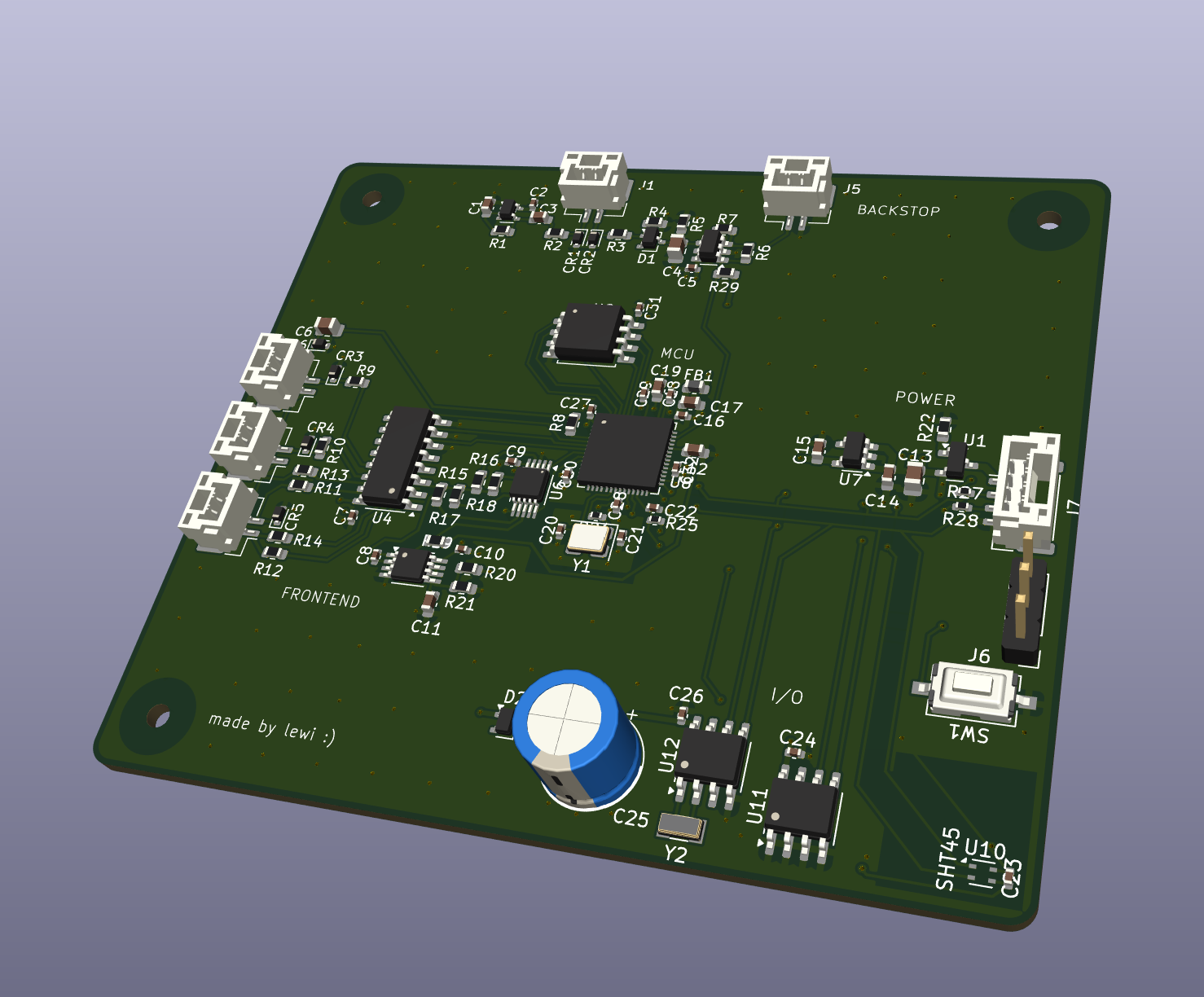 3D View
This was my first mixed-signal PCB layout and my first time using LTspice. Both show.
Commercial leak probes are threshold devices — they answer wet or dry and nothing more. That limitation is physical, not a design shortcut:
You can't measure water with DC. Apply a steady voltage across two electrodes in water and ions pile up on each surface within milliseconds. The reading drifts, and the net DC current slowly dissolves the electrodes.
So you use AC. But no single frequency works.
   LOW frequency   →  the layer of ions on each electrode blocks you
   HIGH frequency  →  the probe cable's own capacitance shunts around
                      the water, and a dry probe reads as flooded
   usable window   →  a few hundred Hz to a few tens of kHz — and the
                      window MOVES depending on how wet the probe is
A second problem, which is why this board has three channels: systems with several enclosures commonly combine their leak sensors into a single alarm bit. You learn something is wet. You don't learn which thing.
A stock BlueROV2 has two watertight enclosures — a 4" electronics tube (the camera lives inside it) and a 3" battery tube — and operators often add a payload tube. ArduSub supports three leak detector instances, which is why this board has three channels. A flooded battery is a power loss and a lithium hazard; a flooded electronics tube is a lost vehicle. Right now both raise the same alarm.
It's also worth being clear about what already exists: every BlueROV2 ships with a hand vacuum pump, and pulling ~15 inHg and watching it for 10–15 minutes is a good pre-dive seal check. But the vacuum is released before the vehicle enters the water, so nothing monitors the seal during the dive. This board addresses the second gap, not the first.
Two independent paths.
   probe 1 ──┐
   probe 2 ──┼──► FRONT END ──────► MCU ────► I²C to the host
   probe 3 ──┘    mux, amplifier,   measures,
                  4 gain ranges     logs, reports

   probe 4 ─────► BACKSTOP ─────────────────► alarm line
                  oscillator, peak            (no firmware
detector, comparator in the path)Excitation. A microcontroller pin swings 0–3.3 V at 10 Hz, 1 kHz or 20 kHz. A 100 Ω resistor softens the edges so the trace doesn't radiate across the board. A 10 µF capacitor in series guarantees zero average current through the water — a capacitor physically cannot pass DC, so the electrodes can't corrode.
Probe interface. Three connectors, one per enclosure. Every wire leaving the board gets a TVS clamp for static protection and a 100 Ω series resistor.
Calibration channels. Three of the multiplexer's inputs go to on-board resistors instead of probes — 100 Ω, 1 kΩ and 1 MΩ. Measuring a known resistor with the same circuit tells you what the circuit itself contributes, so you can subtract it. These are the reason the numbers mean anything.
Multiplexer. An 8:1 switch selects one probe or one calibration reference at a time. This is what preserves per-enclosure identity.
Transimpedance amplifier. The important part. A naive measurement — sense resistor to ground — lets the probe cable steal the signal, because the measuring point moves and the cable charges and discharges following it.
The amplifier instead holds that point perfectly still, pushing back exactly hard enough to keep it from moving. A node that never moves can't charge the cable, so the cable steals nothing. The amount of push-back is the measurement.
In simulation this moved the highest usable frequency from about 1 kHz to about 100 kHz — roughly 100×, and it's what makes the three-frequency scheme possible at all.
Four gain ranges. A flooded probe and a dry probe differ by about 10,000:1. No single amplifier setting reads both, so there are four and firmware picks the one that keeps the reading on scale.
VMID. The board has 0 V and 3.3 V and no negative rail, but the signal needs to swing both ways. So the circuit redefines zero as 1.65 V — a resistor divider buffered by an op-amp. Everything is referenced to that.
A completely separate circuit sharing only the ground plane and the 5 V rail.
  Schmitt oscillator ──► DC block ──► probe ──► divider ──► peak detector ──► comparator
      ~4.5 kHz                                   3.3 kΩ                        TLV3011
A Schmitt-trigger inverter with one resistor and one capacitor oscillates at about 4.5 kHz whenever it has power — no clock, no configuration, nothing to program. A divider turns "how wet" into a voltage, a diode and capacitor turn AC into DC, and a comparator with hysteresis trips at about 2.3 kΩ of probe resistance.
It runs from 5 V, upstream of the 3.3 V regulator. If that regulator fails, the microcontroller dies but the backstop keeps working and can still assert the alarm.
The microcontroller can watch the alarm line to log it. It can't override it.
| Layers | 4 (signal / ground / power / signal), 1.6 mm |
| Size | 75.0 × 65.0 mm |
| JLC04161H-7628 Stackup |
The board was routed using KiCad, and the files can be viewed in /pcb. v1 was made under sleep deprivation. v2 is a more thoughtfully routed board, taking into account proper rule zones, more carefully arranged components, and stricter adherence to the seperation between digital and analog zones.
This has never been built or tested. The full list is in DESIGN.md; the ones that matter most:
| Item | Status |
|---|---|
| Never fabricated | The largest caveat |
| Amplifier compensation on the two high gain ranges | One fixed feedback capacitor can't serve four decades of gain. Needs one per range. Found reviewing my own work; not fixed |
| A broken probe wire reads as "dry" | Nothing distinguishes dry from disconnected. Fix identified — a 10 MΩ across the electrodes at the probe end makes "open" detectable — not implemented |
| Anti-alias filter vs. ADC sample rate | The corner frequency was never chosen against an actual sample rate |
| Electrode material and geometry | Unspecified, and it's what sets the values the whole frequency analysis rests on |
| Interference from nearby motor drives | Not analysed |
  /schematics     KiCad schematics, 5 sheets, plus PDFs
  /pcb            KiCad layout, 4 layers, renders
  /sim            LTspice files for the front end and backstop
DESIGN.md full design document, every decision and whyI've tried to be exact about which values are sourced and which are assumptions. Several are assumptions.
| Quantity | Value used | Source |
|---|---|---|
| Equivalent circuit model | Randles cell (solution resistance in series with a parallel double-layer capacitance and charge-transfer resistance) | Randles, J.E.B., Kinetics of rapid electrode reactions, Discussions of the Faraday Society, vol. 1, 1947. Modern summary: Gamry, Basics of EIS |
| Double-layer capacitance | 0.5 µF per electrode | Derived, not measured. Gamry gives 20–60 µF/cm² for a metal–electrolyte interface. 0.5 µF therefore implies roughly 1 mm² of wetted electrode area. A realistic probe with larger pads would have a considerably higher Cdl, which shifts the low-frequency limit — see Open items |
| Charge-transfer resistance | 100 kΩ | Order-of-magnitude placeholder. Not sourced. It depends on electrode material, surface condition and water chemistry, none of which are specified in this design |
| Quantity | Value used | Source |
|---|---|---|
| Probe cable capacitance | 200 pF | Estimate. TI, A Practical Guide to Cable Selection (SNLA164) cites 12–16 pF/ft (≈39–52 pF/m) mutual capacitance for low-capacitance twisted pair. 200 pF corresponds to roughly a 4 m run, or less for ordinary PVC-insulated pairs. Assumption, not a measurement of a specific cable |
This project was a way to further my experience with ECAD, as well as learn how analog design decisions get made.
The schematic capture and the PCB layout work are mine, and that's where most of the hours went.
The design decisions were largely not mine, and I feel that I should be honest about that. I worked through this with Claude (Anthropic), which proposed the architecture - the three-tone excitation scheme, the transimpedance front end, the switched gain ranges, the calibration channels, and the backstop - recommended the component families (verified by me), wrote the LTspice exercises I learned to simulate from, and wrote this documentation.
I haven't taken the advanced analog electronics sequence yet, but I feel that this was a good start into analog design. It wasn't my most refined project, and I do think I could have owned more of the design itself, but it definitely motivated me to independently explore analog electronics further.
Also thank you to Altium Academy, whose mixed-signal layout videos were very helpful, and to the KiCad project, whose libraries saved me a lot of effort importing components.
| Qty | Value | Footprint | References |
|---|---|---|---|
| 13 | 100nF | Capacitor_SMD:C_0402_1005Metric | C2, C5, C7, C9, C10, C16, C18, C22, C23, C24, C26, C27, C28 |
| 8 | 100 | Resistor_SMD:R_0603_1608Metric | R2, R3, R8, R9, R10, R11, R12, R18 |
| 6 | 1uF | Capacitor_SMD:C_0603_1608Metric | C3, C11, C14, C15, C17, C19 |
| 6 | PESD5V0S1BA | Diode_SMD:D_SOD-523 | CR1, CR2, CR3, CR4, CR5, CR6 |
| 5 | Conn_01x02_Pin | Connector_JST:JST_GH_BM02B-GHS-TBT_1x02-1MP_P1.25mm_Vertical | J1, J2, J3, J4, J5 |
| 3 | 10k | Resistor_SMD:R_0603_1608Metric | R20, R21, R29 |
| 2 | 100k | Resistor_SMD:R_0603_1608Metric | R16, R22 |
| 2 | 10uF | Capacitor_SMD:C_0805_2012Metric | C6, C13 |
| 2 | 15pF | Capacitor_SMD:C_0402_1005Metric | C20, C21 |
| 2 | 1M | Resistor_SMD:R_0603_1608Metric | R5, R13 |
| 2 | 1k | Resistor_SMD:R_0603_1608Metric | R14, R19 |
| 2 | 4.7k | Resistor_SMD:R_0402_1005Metric | R27, R28 |
| 2 | 47k | Resistor_SMD:R_0603_1608Metric | R1, R7 |
| 2 | BAT54W | Package_TO_SOT_SMD:SOT-323_SC-70 | D1, D2 |
| 1 | 0.1F | Capacitor_THT:CP_Radial_D8.0mm_P3.50mm | C25 |
| 1 | 100nF | Capacitor_SMD:C_0805_2012Metric | C4 |
| 1 | 10k | Resistor_SMD:R_0402_1005Metric | R25 |
| 1 | 12MHz | Crystal:Crystal_SMD_3225-4Pin_3.2x2.5mm | Y1 |
| 1 | 1k | Resistor_SMD:R_0402_1005Metric | R24 |
| 1 | 1nF | Capacitor_SMD:C_0603_1608Metric | C12 |
| 1 | 2.2M | Resistor_SMD:R_0603_1608Metric | R6 |
| 1 | 2.2pF | Capacitor_SMD:C_0402_1005Metric | C8 |
| 1 | 3.3k | Resistor_SMD:R_0603_1608Metric | R4 |
| 1 | 32.768 kHz | Crystal:Crystal_SMD_3215-2Pin_3.2x1.5mm | Y2 |
| 1 | 3M | Resistor_SMD:R_0603_1608Metric | R15 |
| 1 | 3k | Resistor_SMD:R_0603_1608Metric | R17 |
| 1 | 4.7nF | Capacitor_SMD:C_0603_1608Metric | C1 |
| 1 | 600R @ 100MHz | Inductor_SMD:L_0603_1608Metric | FB1 |
| 1 | 74LVC1G14 | Package_TO_SOT_SMD:SOT-353_SC-70-5 | U2 |
| 1 | AP2112K-3.3 | Package_TO_SOT_SMD:SOT-23-5 | U7 |
| 1 | CD4051B | Package_SO:SOIC-16_3.9x9.9mm_P1.27mm | U4 |
| 1 | Conn_01x03_Pin | Connector_PinHeader_2.54mm:PinHeader_1x03_P2.54mm_Vertical | J6 |
| 1 | Conn_01x04_Pin | Connector_JST:JST_GH_BM04B-GHS-TBT_1x04-1MP_P1.25mm_Vertical | J7 |
| 1 | DMG3415U-7 | Package_TO_SOT_SMD:SOT-23 | U1 |
| 1 | MB85RC64 | Package_SO:SOIC-8_3.9x4.9mm_P1.27mm | U11 |
| 1 | OPA2333xxD | Package_SO:MSOP-8_3x3mm_P0.65mm | U5 |
| 1 | PCF8563T | Package_SO:SOIC-8_3.9x4.9mm_P1.27mm | U12 |
| 1 | RP2040 | Package_DFN_QFN:QFN-56-1EP_7x7mm_P0.4mm_EP3.2x3.2mm | U8 |
| 1 | SHT45 | Sensor_Humidity:Sensirion_DFN-4_1.5x1.5mm_P0.8mm_SHT4x_NoCentralPad | U10 |
| 1 | SW_MEC_5G | Button_Switch_SMD:SW_SPST_TL3342 | SW2 |
| 1 | TLV3011AIDBVT | Package_TO_SOT_SMD:SOT-23-6 | U3 |
| 1 | TMUX1104DGSR | Package_SO:VSSOP-10_3x3mm_P0.5mm | U6 |
| 1 | W25Q128JVSIQ | Package_SO:SOIC-8_5.3x5.3mm_P1.27mm | U9 |
The 86 most common of 90 parts.
jadenrhee/wigglecam-controller
RP2040 co-processor board for a 4-lens wigglegram camera: constant-current flash, controls, battery telemetry, Pi 5 I2C interface. 4-layer, DRC-clean, fab-ready.


TheCacophonyProject/thermal-camera-v2
tc2-panel.py uses KiKit to build the manufacturing panel from the individual board files.


It measures 73.6 × 59.8 mm and has 4 copper layers, 1.61 mm thick.
90 parts, built around the RP2040, W25Q128JVSIQ, 74LVC1G14Z and AP2112K-3.3. The full list of its parts is on this page, with links to each part's symbol and footprint where PCBKit's library has them.
From the lewipewi/leakwatch repository on GitHub, at the commit this page was made from: the board is pcb/leak_sensor_v1.kicad_pcb and its schematic schematics/backstop.kicad_sch. PCBKit opens the board in the browser, with nothing to install.
Its repository states no licence, so its author keeps all rights: ask lewipewi before reusing the design.