4 layers193 × 105.2 mm
AFE V3
Pgr18/CELL_Z_SPECT_hardware
Печатные платы для проекта клеточной импедансной спектроскопии
293 parts

 koggertech/Kogger_UART_WiFi_Bridge1
Open-source ESP32-C3 UART to Wi-Fi bridge: firmware (ESP-IDF), KiCad 10 board, datasheet. Two UART lines relayed to UDP/TCP as whole frames, station or AP with DHCP, control over Kogger SBP, OTA with rollback.
WiFi UART Bridge v3 is an open-source printed circuit board by koggertech, from the koggertech/Kogger_UART_WiFi_Bridge repository on GitHub, published under the MIT licence. It is a 4-layer board of 20 × 30 mm with 41 parts on 32 nets, routed with 561 tracks and 82 vias.
It is built around the ESP32-C3-MINI-1U-H4, LMZM23601V3SILR and BAS 3005B-02V H6327, with the CL21A226MAYNNNE, SDM4A40EP3-7B and SM04B-GHS-TB(LF)(SN) among its other parts. Its parts include 12 diodes, 11 resistors, 8 capacitors, 2 ICs and 2 crystals. It belongs with the interfaces and adapters and radio and wireless boards and the ESP32 and RISC-V boards of this library.


KiCad 10 project of the reference board, the board that was manufactured and is in use. Every drill hole and every solder‑paste opening of this board matches the fabrication files the board was made from (checked, see below).
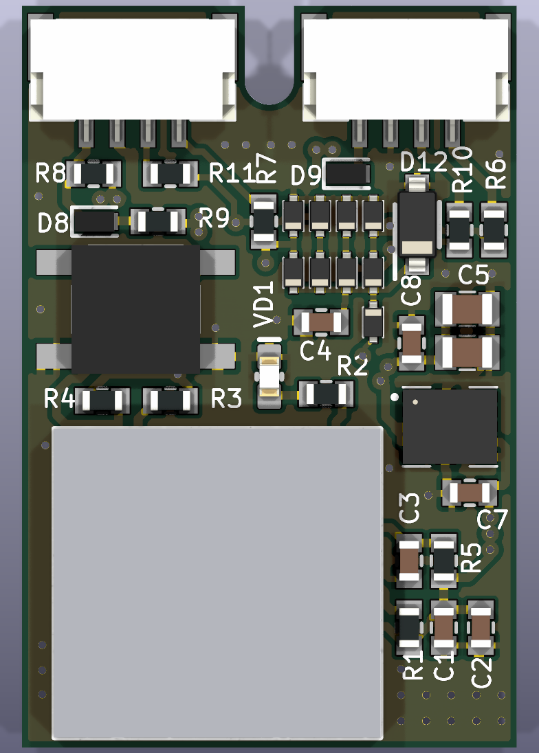
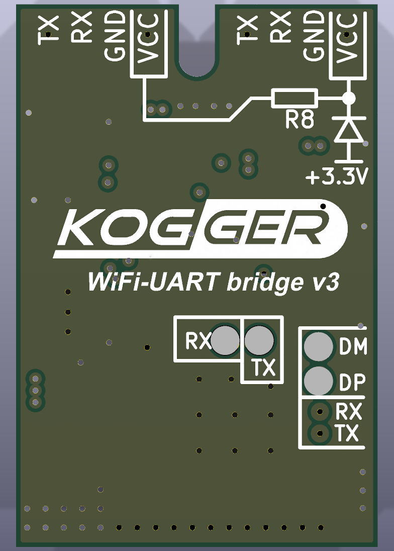
| File | Contents |
|---|---|
WiFi_UART_Bridge_v3.kicad_pro | project (open this in KiCad 10 or later) |
WiFi_UART_Bridge_v3.kicad_sch | schematic, one A4 sheet |
WiFi_UART_Bridge_v3.kicad_pcb | board: 20 × 30 mm, 4 layers |
WiFi_UART_Bridge.kicad_sym, WiFi_UART_Bridge.pretty/ | project symbol and footprint libraries (sym-lib-table, fp-lib-table) |
3d/ | plain box bodies for renders (module, switch, 4 A diodes); other parts use KiCad library models |
outputs/WiFi_UART_Bridge_v3_schematic.pdf | schematic |
outputs/WiFi_UART_Bridge_v3_fab.zip | Gerbers, Excellon drill, drill map, Gerber job file, pick‑and‑place, BOM |
outputs/WiFi_UART_Bridge_v3_bom.csv, _pos.csv | BOM and pick‑and‑place (top side, mm, origin at the lower‑left board corner) |
The outputs are generated by python tools/make_hw_outputs.py (needs kicad-cli of KiCad 10).
| Size | 20 × 30 mm, a 2 mm wide, 4 mm deep notch with a rounded end between the two connectors |
| PCB | 4 layers, FR4 1.2 mm, 18 µm copper, ENIG finish, green solder mask, white silkscreen |
| Stackup in the file | nominal: 0.2 mm prepreg, 0.708 mm core, 0.2 mm prepreg; use the fab's standard 1.2 mm 4‑layer stackup |
| Layers | F.Cu: signals and GND pour; In1.Cu: GND; In2.Cu: VCC, +3.3 V and UART routing plus a GND pour; B.Cu: GND pour and the test pads |
| Design rules | track 0.2 mm min, clearance 0.2 mm, vias 0.7/0.3 mm (82), copper to edge 0.25 mm |
| Components | 37 on the top side; 4 test pads on the bottom |
| Connector | Pin 1 | Pin 2 | Pin 3 | Pin 4 |
|---|---|---|---|---|
| X1 (line 0) | TX (GPIO21) | RX (GPIO20) | GND | VCC in (through D9) |
| X2 (line 1) | TX (GPIO5) | RX (GPIO4) | GND | VCC_X2 |
X1 and X2 are JST GH 4‑pin headers, 1.25 mm, right angle (SM04B‑GHS‑TB). The mating housing is GHR‑04V‑S. The bottom silkscreen names the pins.
Changes to the content of the original design, all visible in the files:
The hardware design files are published under the same MIT license as the rest of the repository
(../LICENSE). KiCad library symbols embedded in the schematic, the symbol VCC_X2 of the project library
(derived from KiCad power:VCC) and the KiCad 3D models the board refers to are covered by the KiCad libraries'
license (../THIRD_PARTY.md).
The KOGGER logo on the bottom silkscreen of the board is not licensed under the MIT License. The fab zip in
hardware/outputs includes it: before making boards that KOGGER LLC does not supply, delete the logo from B.SilkS
and regenerate the outputs with tools/make_hw_outputs.py.
| Qty | Value | Footprint | References |
|---|---|---|---|
| 9 | BAS3005B-02V | WiFi_UART_Bridge:D_SC-79 | D1, D3, D4, D6, D7, D10, D11, D13, D14 |
| 4 | 10k | WiFi_UART_Bridge:R_0603_1608Metric_Big | R1, R3, R4, R5 |
| 3 | 0.1uF | WiFi_UART_Bridge:C_0603_1608Metric_Big | C2, C4, C8 |
| 3 | 1k | WiFi_UART_Bridge:R_0603_1608Metric_Big | R2, R10, R11 |
| 2 | 0 | WiFi_UART_Bridge:R_0603_1608Metric_Big | R8, R9 |
| 2 | 10uF | WiFi_UART_Bridge:C_0603_1608Metric_Big | C1, C7 |
| 2 | 150 | WiFi_UART_Bridge:R_0603_1608Metric_Big | R6, R7 |
| 2 | 22uF | WiFi_UART_Bridge:C_0805_2012Metric | C5, C6 |
| 2 | SDM4A40EP3 | WiFi_UART_Bridge:D_SDM4A40EP3 | D8, D9 |
| 2 | SM04B-GHS-TB | WiFi_UART_Bridge:JST_GH_SM04B-GHS-TB_1x04-1MP_P1.25mm_Horizontal | X1, X2 |
| 1 | 1uF | WiFi_UART_Bridge:C_0603_1608Metric_Big | C3 |
| 1 | DM | WiFi_UART_Bridge:TestPoint_Pad_D1.6mm | TP1 |
| 1 | DP | WiFi_UART_Bridge:TestPoint_Pad_D1.6mm | TP2 |
| 1 | ESP32-C3-MINI-1U | WiFi_UART_Bridge:ESP32-C3-MINI-1U | U1 |
| 1 | LED green | WiFi_UART_Bridge:LED_0603_1608Metric | VD1 |
| 1 | LMZM23601V3 | WiFi_UART_Bridge:TI_SIL0010A_LMZM2360x | U2 |
| 1 | MMSZ5226B | WiFi_UART_Bridge:D_SOD-123 | D12 |
| 1 | PTS525SM15SMTR2 | WiFi_UART_Bridge:SW_CK_PTS525SM15SMTR2 | SB1 |
| 1 | RX | WiFi_UART_Bridge:TestPoint_Pad_D1.6mm | TP4 |
| 1 | TX | WiFi_UART_Bridge:TestPoint_Pad_D1.6mm | TP3 |
Pgr18/CELL_Z_SPECT_hardware
Печатные платы для проекта клеточной импедансной спектроскопии

OliviezGit/FC_01
Le dossier composants contient les fiches techniques PDF, bibliothèques locales, STEP, vues de contrôle et la nomenclature France du 27/09/2026.


jeis-aj/PORTABLE-ECG
A Handheld ECG Machine with Mobile phone and Laptop interface. Cardiac condition prediction using ML

millerlp/BivalveBit_hardware
Heart rate and valve gape sensor wearable for oysters and mussels

Paschalis/Hardware-Login-Key
The Hardware Login Key is an ATtiny85-based USB device that securely automates password entry using a physical button or touch sensor. It offers a simple, hardware-driven way to log into systems or websites.


Adityawadpalliwar/smart-hydration-reminder-PCB
A compact, low-power, wireless-capable PCB designed to live in a water bottle base or sleeve. It detects when you drink using a 6-axis IMU, keeps a running record of intake events, and reminds you with a buzzer when you…
It measures 20 × 30 mm and has 4 copper layers, 1.2 mm thick.
41 parts, built around the ESP32-C3-MINI-1U-H4, LMZM23601V3SILR, BAS 3005B-02V H6327 and CL21A226MAYNNNE. The full list of its parts is on this page, with links to each part's symbol and footprint where PCBKit's library has them.
From the koggertech/Kogger_UART_WiFi_Bridge repository on GitHub, at the commit this page was made from: the board is hardware/WiFi_UART_Bridge_v3.kicad_pcb and its schematic hardware/WiFi_UART_Bridge_v3.kicad_sch. PCBKit opens the board in the browser, with nothing to install.
Its repository publishes it under the MIT licence: you may reuse it on that licence's terms (keep the author's notice, and for a copyleft licence share your changes alike).