4 layers252 × 152 mm
CTA control board
PySpice-org/eda-rw
Python library to read/write KiCad and LibrePCB Sexpr file format
619 parts9

 kardTaczka/easter_pcb
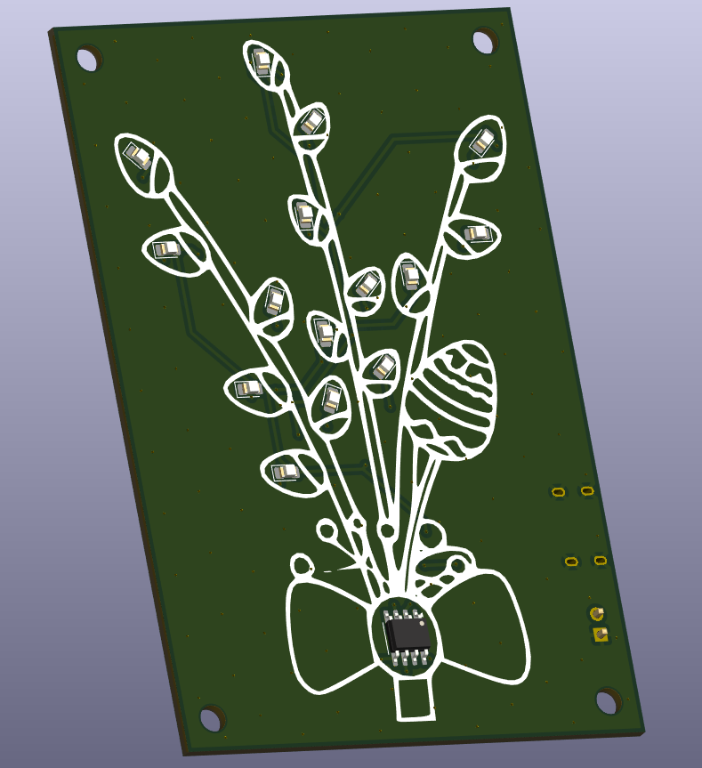
For soldering learning. 15 leds connected to breathing 555. Frequency around 0.2 Hz for smooth breathing-like behaviour.
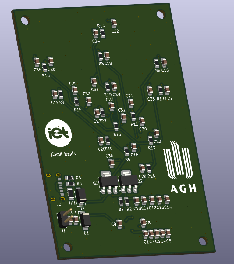
Palemka is an open-source printed circuit board by kardTaczka, from the kardTaczka/easter_pcb repository on GitHub. It is a 2-layer board of 60 × 90 mm with 86 parts on 29 nets, routed with 301 tracks and 152 vias.
It is built around the NE555P, SM5059 and BCP53, with the BCP56 among its other parts. Its parts include 37 capacitors, 19 resistors, 17 diodes, 2 transistors and 2 connectors.


Below are presented screenshots of 3d render PCB and schematic.
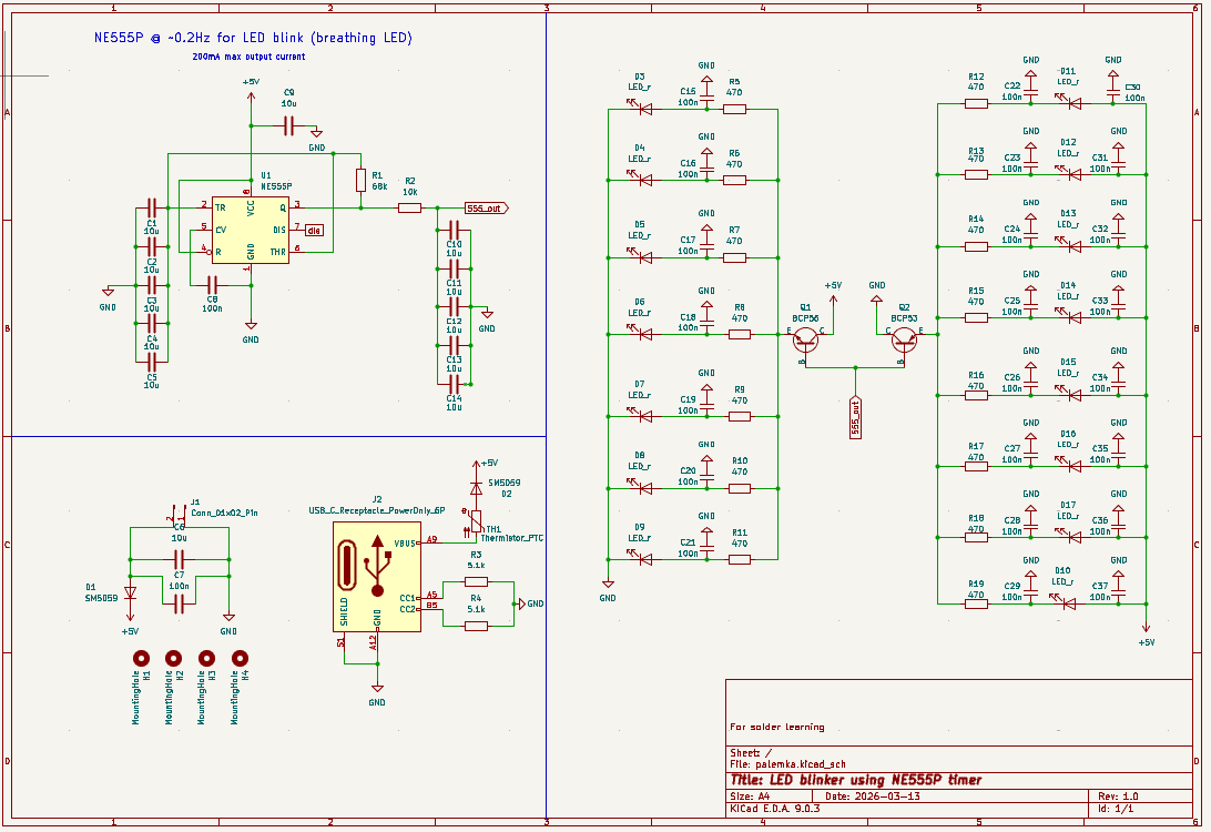
Dual-Channel Alternating Output - The NE555 timer operates at approximately 0.2 Hz. Its square wave output is smoothed by an RC integration network consisting of a 10 kΩ resistor and a 50 µF capacitor bank (achieved by placing five 10 µF MLCCs in parallel). This analog signal drives a complementary transistor pair consisting of a BCP56 (NPN) and a BCP53 (PNP).
Instead of driving a single array, the load is split into two separate LED rails. Because the NPN and PNP transistors conduct on opposite voltage swings, they create an alternating "breathing" effect. When the capacitor charges, the NPN rail fades in while the PNP rail fades out. When the voltage drops, the cycle reverses. The peak forward current is hardware-limited to a safe and visually pleasing 3 mA per LED.
| Qty | Value | Footprint | References |
|---|---|---|---|
| 25 | 100n | Capacitor_SMD:C_0805_2012Metric_Pad1.18x1.45mm_HandSolder | C15, C16, C17, C18, C19, C20, C21, C22, C23, C24, C25, C26, C27, C28, C29, C30 +9 |
| 15 | 470 | Resistor_SMD:R_0805_2012Metric_Pad1.20x1.40mm_HandSolder | R5, R6, R7, R8, R9, R10, R11, R12, R13, R14, R15, R16, R17, R18, R19 |
| 15 | LED_r | LED_SMD:LED_0805_2012Metric_Pad1.15x1.40mm_HandSolder | D3, D4, D5, D6, D7, D8, D9, D10, D11, D12, D13, D14, D15, D16, D17 |
| 12 | 10u | Capacitor_SMD:C_0805_2012Metric_Pad1.18x1.45mm_HandSolder | C1, C2, C3, C4, C5, C6, C9, C10, C11, C12, C13, C14 |
| 4 | MountingHole | MountingHole:MountingHole_3.2mm_M3 | H1, H2, H3, H4 |
| 3 | LOGO | LOGO | G***, G***, G*** |
| 2 | 5.1k | Resistor_SMD:R_0805_2012Metric_Pad1.20x1.40mm_HandSolder | R3, R4 |
| 2 | SM5059 | Diode_SMD:D_SMA | D1, D2 |
| 1 | 10k | Resistor_SMD:R_0805_2012Metric_Pad1.20x1.40mm_HandSolder | R2 |
| 1 | 68k | Resistor_SMD:R_0805_2012Metric_Pad1.20x1.40mm_HandSolder | R1 |
| 1 | BCP53 | Package_TO_SOT_SMD:SOT-223 | Q2 |
| 1 | BCP56 | Package_TO_SOT_SMD:SOT-223 | Q1 |
| 1 | Conn_01x02_Pin | Connector_PinHeader_2.54mm:PinHeader_1x02_P2.54mm_Vertical | J1 |
| 1 | NE555P | Package_SO:SOIC-8_3.9x4.9mm_P1.27mm | U1 |
| 1 | Thermistor_PTC | Resistor_SMD:R_1206_3216Metric_Pad1.30x1.75mm_HandSolder | TH1 |
| 1 | USB_C_Receptacle_PowerOnly_6P | palemka:usb4970 | J2 |
It measures 60 × 90 mm and has 2 copper layers, 1.6 mm thick.
86 parts, built around the NE555P, SM5059, BCP53 and BCP56. The full list of its parts is on this page, with links to each part's symbol and footprint where PCBKit's library has them.
From the kardTaczka/easter_pcb repository on GitHub, at the commit this page was made from: the board is palemka.kicad_pcb and its schematic palemka.kicad_sch. PCBKit opens the board in the browser, with nothing to install.
Its repository states no licence, so its author keeps all rights: ask kardTaczka before reusing the design.
PySpice-org/eda-rw
Python library to read/write KiCad and LibrePCB Sexpr file format


damianmoore/wifi-lamp
A simple wifi-enabled lamp control board based on the ESP8266

Emile666/Brew_Hardware_STM8S207
Brewing hardware with STM8S207, Kicad project

Cosmas-cmd/STM32F407VGTX-DEVELOPMENT-BOARD
A custom STM32F407VGTx development board designed in KiCad 9.0, featuring the STM32F407 (LQFP100, Cortex-M4F @ 168 MHz) with an external crystal, USB Type-C power input, onboard microSD card and much more...

Adamos-khalilos/stm32f407VGTx-dev-board-PCB-
A custom STM32F407VGTx development board featuring a microSD card slot, SWD debug header, wake-up button, RGB status LEDs, and a clean decoupled power supply. Designed entirely in KiCad.
