
4 layers144 × 150 mm

 k-takata/PCB_USB_C_for_breadboard1
USB Type-C Power Adaptor for Breadboard
PCB USB C for breadboard is an open-source printed circuit board by k-takata, from the k-takata/PCB_USB_C_for_breadboard repository on GitHub. It is a 2-layer board of 21.3 × 18 mm with 14 parts on 14 nets, routed with 81 tracks and 2 vias.
It is built around the LM1117GS-3.3. Its parts include 5 connectors, 3 resistors, 2 fuses, 1 capacitor and 1 IC.
USB Type-Cからブレッドボードに電源を供給するためのアダプターです。 供給電圧は5Vと3.3Vをジャンパーピンで選択できます。
KiCad 9.0
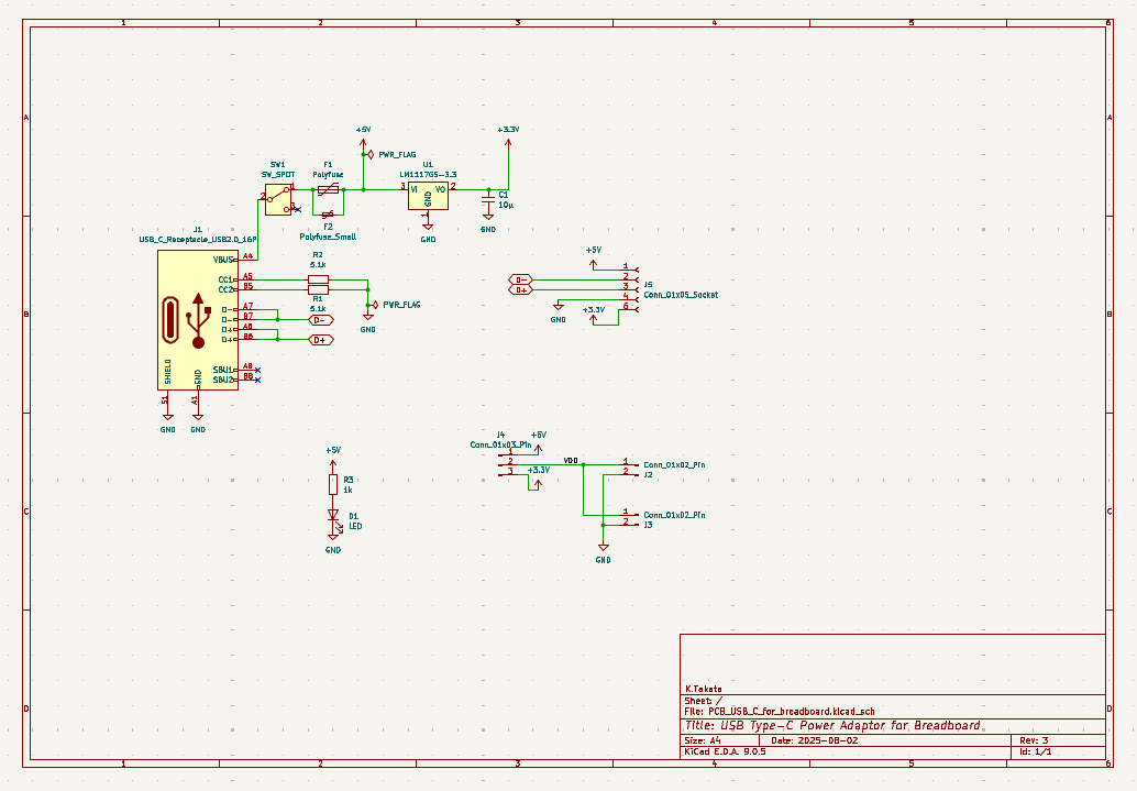
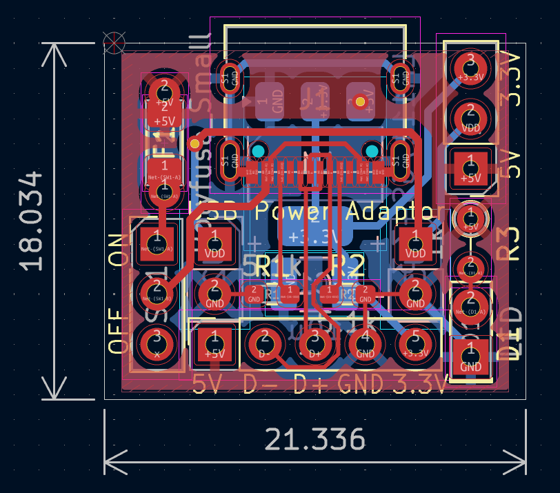
| Reference | 個数 | 値 | 説明 |
|---|---|---|---|
| C1 | 1 | 10μF | 積層セラミックコンデンサー 3225M |
| D1 | 1 | 角形LED (あるいは3mm LEDや1608MチップLED) | |
| F1 (*1) | 1 | 1.1A | ポリヒューズ |
| F2 (*1) | 1 | 0.5A | ポリヒューズ、表面実装 |
| J1 | 1 | USB Type-Cコネクター | |
| J2, J3 | 2 | 細ピンヘッダー 1x2、ブレッドボードへの挿入用、裏面に取り付け | |
| J4 | 1 | ピンヘッダー 1x3、出力電圧設定用 | |
| J5 | 1 | ピンソケット 1x5 | |
| R1, R2 | 2 | 5.1kΩ | 1608M |
| R3 | 1 | 1kΩ | 1/6Wまたは1/4W、LED電流制限用。値はLEDや好みの明るさに応じて適宜調整 (1kΩ~47kΩ) |
| SW1 | 1 | スライドスイッチ | |
| U1 (*2) | 1 | LM1117GS-3.3 | 三端子レギュレーター 3.3V 1A |
注:
以下の順で取り付けるのがお勧めです。
J5とSW1は少し干渉するので、J5を少し削る必要があるかもしれません。
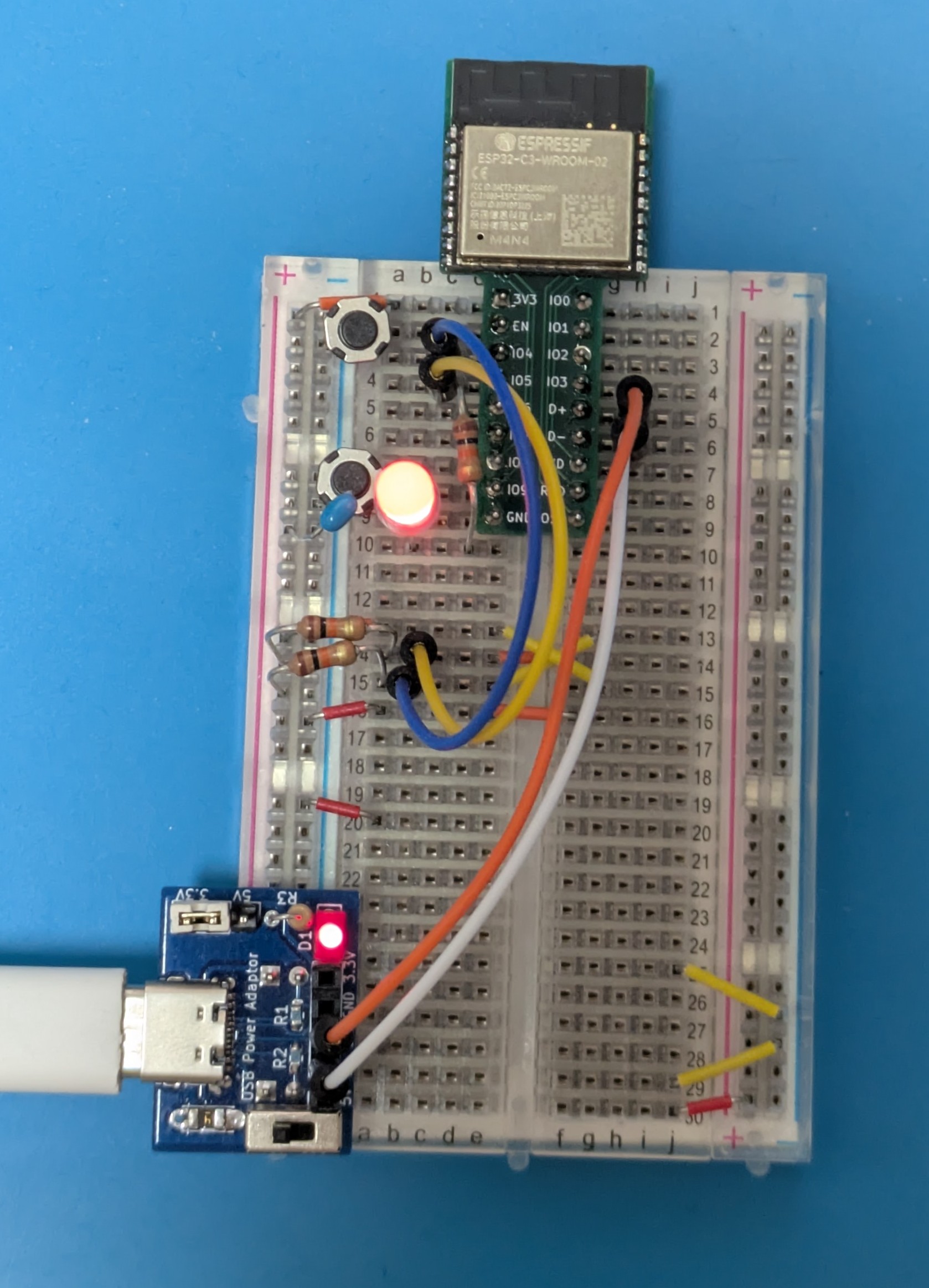
基板裏面に取り付けたピンヘッダーJ2, J3をブレッドボードの電源ラインに挿入して使用します。J2, J3に供給する電圧はJ4にジャンパーピンを挿すことで5Vあるいは3.3Vから選択します。
J2, J3の端子は、USBコネクター側がプラス (シルクにはVDDあるいは+の表示)、反対側がマイナス (シルクにはGNDあるいは-の表示)です。向きに注意してください。
SW1が電源スイッチです。電源がオンになっていれば、LEDが点灯します。
5Vと3.3Vの両方を使用したい場合や、D+/D-のデータ線を使用したい場合は、J5にコードを接続して使います。
Rev. 1
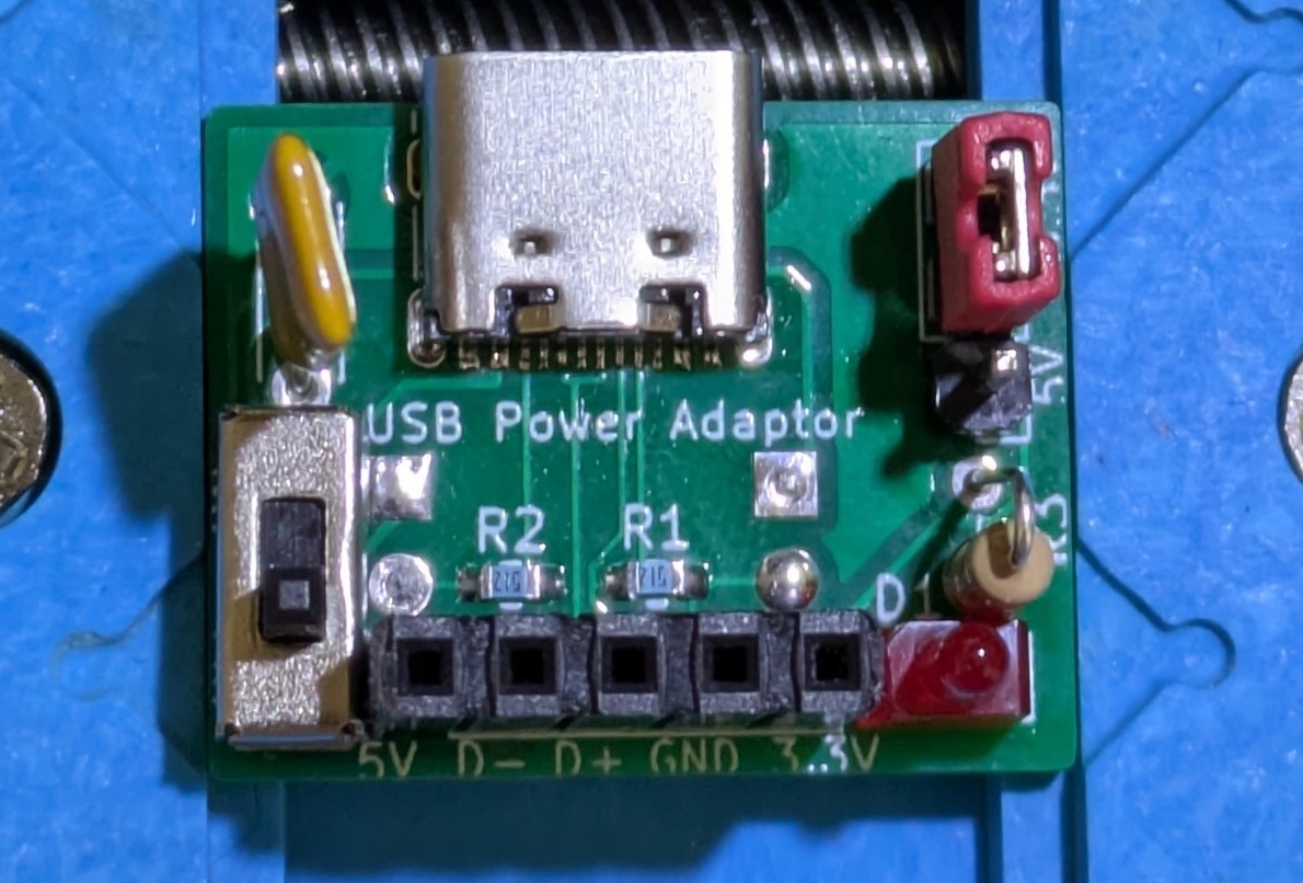
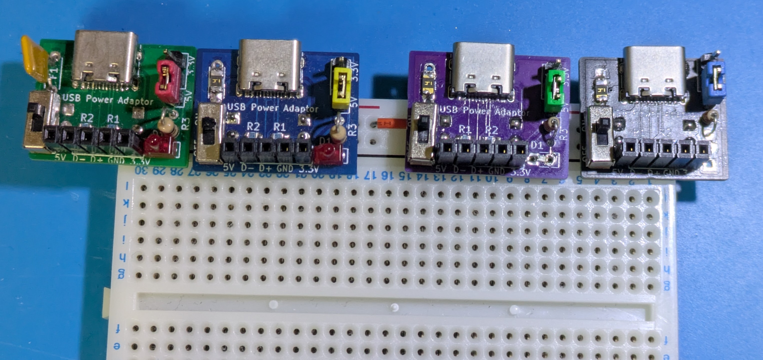
左から順にRev. 1, Rev. 2, Rev. 3
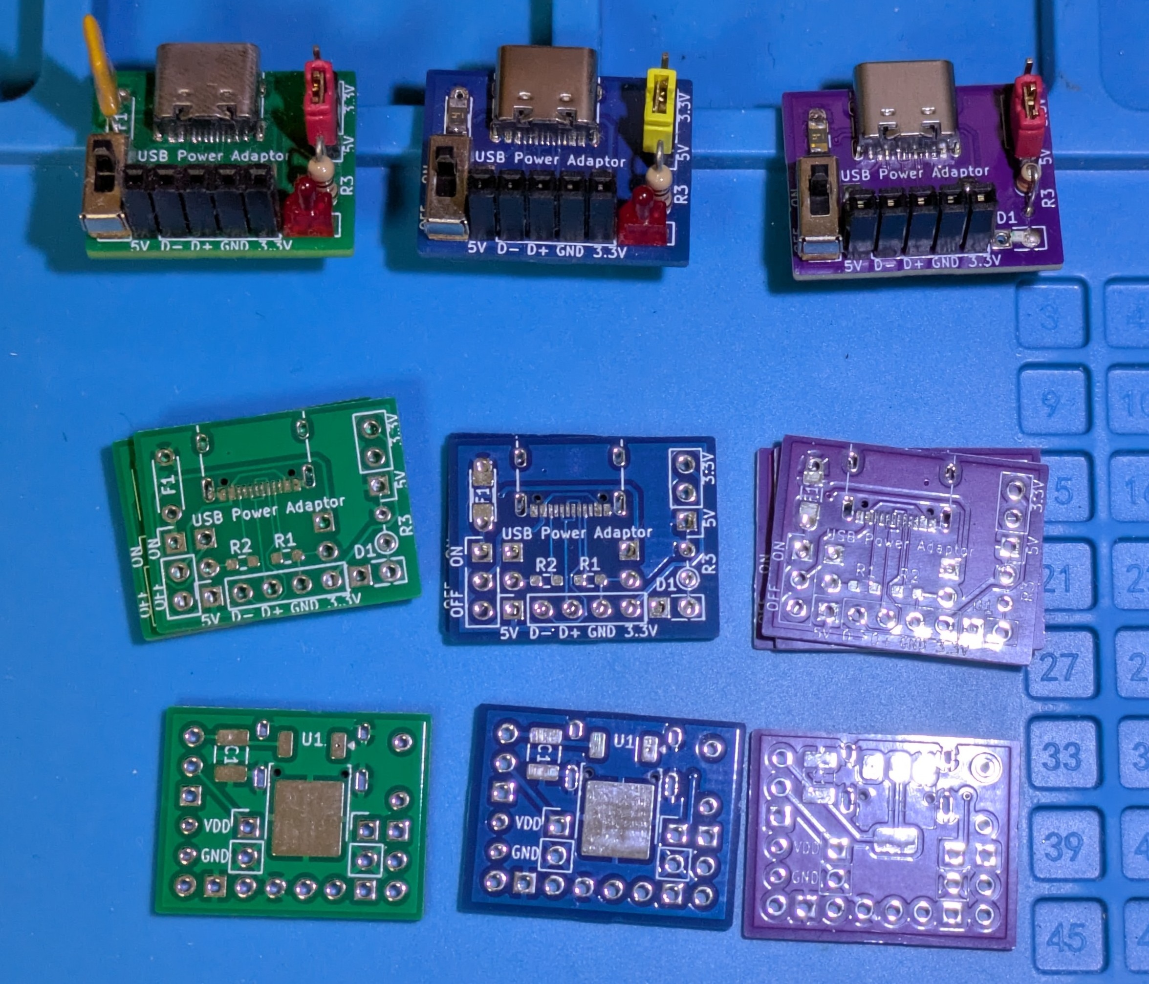
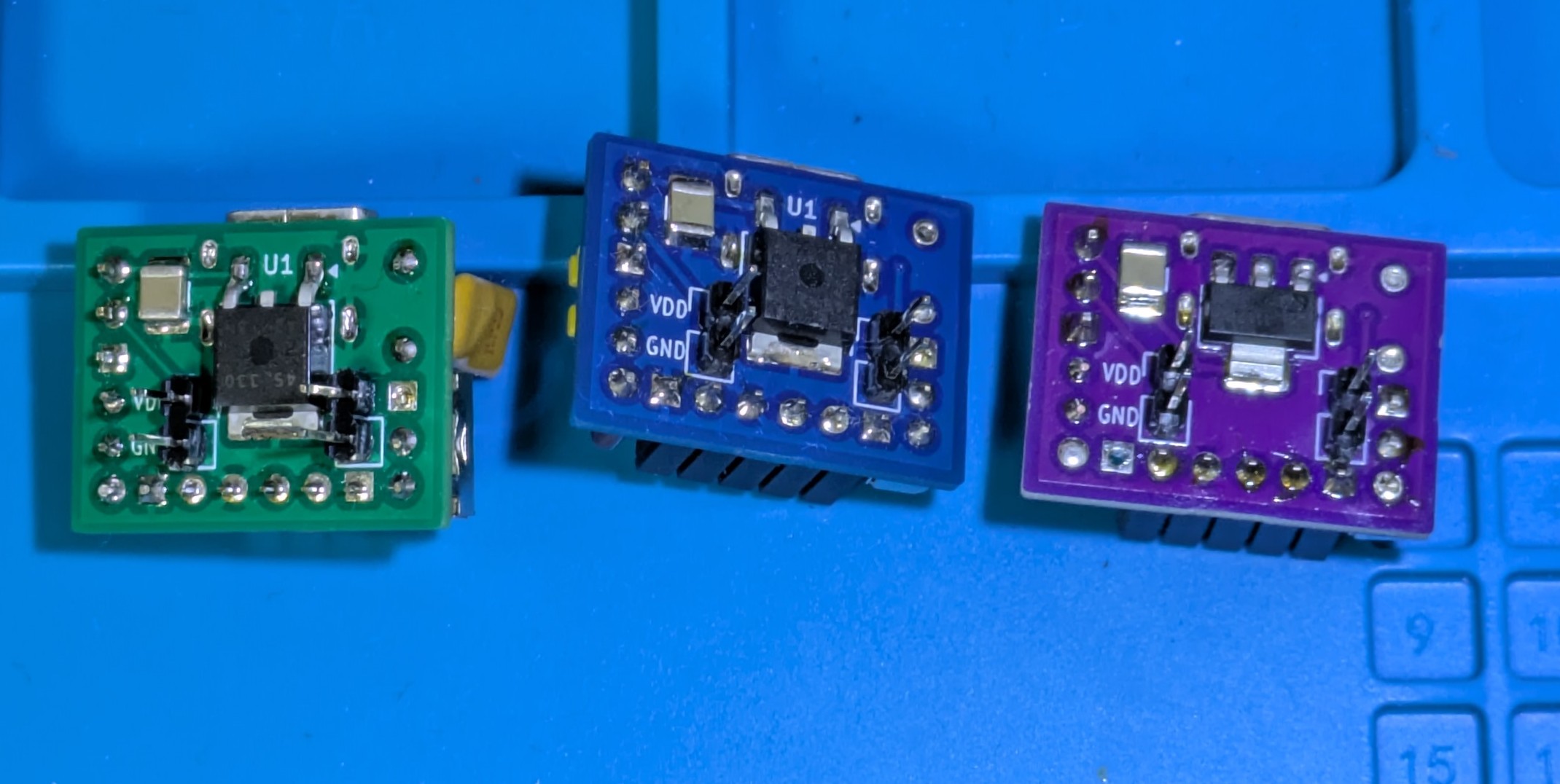
Rev. 1, Rev. 2, Rev. 3の裏面
左から順にRev. 1, Rev. 2, Rev. 3, Rev. 4
ブレッドボードに挿して使用している例 (ESP32-C3-WROOM-02 Breakout Boardとともに)
CC0
| Qty | Value | Footprint | References |
|---|---|---|---|
| 2 | 5.1k | Resistor_SMD:R_0603_1608Metric_Pad0.98x0.95mm_HandSolder | R1, R2 |
| 2 | Conn_01x02_Pin | Connector_PinHeader_2.54mm:PinHeader_1x02_P2.54mm_Vertical | J2, J3 |
| 1 | 10μ | Capacitor_SMD:C_1210_3225Metric_Pad1.33x2.70mm_HandSolder | C1 |
| 1 | 1k | Resistor_THT:R_Axial_DIN0204_L3.6mm_D1.6mm_P2.54mm_Vertical | R3 |
| 1 | Conn_01x03_Pin | Connector_PinHeader_2.54mm:PinHeader_1x03_P2.54mm_Vertical | J4 |
| 1 | Conn_01x05_Socket | Connector_PinSocket_2.54mm:PinSocket_1x05_P2.54mm_Vertical | J5 |
| 1 | LED | LED_THT:LED_Rectangular_W5.0mm_H2.0mm | D1 |
| 1 | LM1117GS-3.3 | Package_TO_SOT_SMD:SOT-223-3_TabPin2 | U1 |
| 1 | Polyfuse | Capacitor_THT:C_Disc_D4.3mm_W1.9mm_P5.00mm | F1 |
| 1 | Polyfuse_Small | Fuse:Fuse_1206_3216Metric_Pad1.42x1.75mm_HandSolder | F2 |
| 1 | SW_SPDT | Connector_PinHeader_2.54mm:PinHeader_1x03_P2.54mm_Vertical | SW1 |
| 1 | USB_C_Receptacle_USB2.0_16P | Connector_USB:USB_C_Receptacle_XKB_U262-16XN-4BVC11 | J1 |


It measures 21.3 × 18 mm and has 2 copper layers, 1.2 mm thick.
14 parts, built around the LM1117GS-3.3. The full list of its parts is on this page, with links to each part's symbol and footprint where PCBKit's library has them.
From the k-takata/PCB_USB_C_for_breadboard repository on GitHub, at the commit this page was made from: the board is PCB_USB_C_for_breadboard.kicad_pcb and its schematic PCB_USB_C_for_breadboard.kicad_sch. PCBKit opens the board in the browser, with nothing to install.
Its repository states no licence, so its author keeps all rights: ask k-takata before reusing the design.