2 layers27.9 × 16.5 mm

 jrleeman/I2CPullupBreakout
Prototyping aid that allows selectable pull-up and series resistors for the I2C bus
I2CPullupBreakout is an open-source printed circuit board by jrleeman, from the jrleeman/I2CPullupBreakout repository on GitHub. It is a 2-layer board of 33 × 24.4 mm with 18 parts on 17 nets, routed with 102 tracks and 2 vias.
Its parts include 12 resistors and 5 connectors.
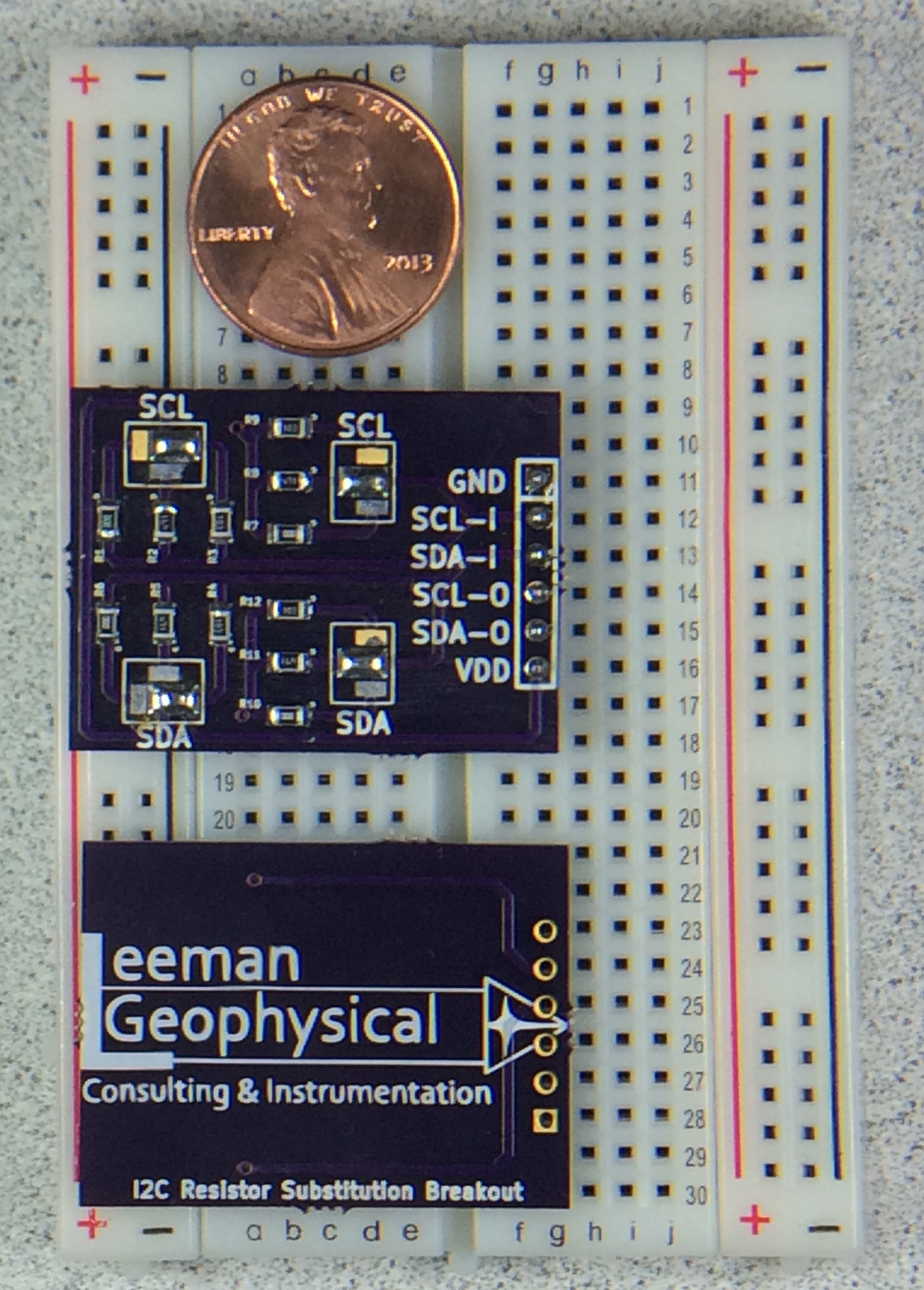
Prototyping aid that allows selectable pull-up and series resistors for the I2C bus. To use, just insert the module into your circuit/breadboard and select the appropriate series/pull up resistor values with the solder jumpers. Bridging the jumpers is very easy and switching usually just requires a swipe with the soldering iron.
The I2C Pullup Breakout is available through Leeman Geophysical by emailing John R. Leeman at kd5wxb@gmail.com.
This repository includes all design information, CAD files, PDF CAD output, gerbers, etc.
Additional resources for this project include:
This product is licenced under the CERN Open Hardware License 1.2. The full license is included in this repository.
| Qty | Value | Footprint | References |
|---|---|---|---|
| 4 | 0 | SM0805 | R1, R6, R7, R10 |
| 4 | 10K | SM0805 | R3, R4, R9, R12 |
| 4 | 470 | SM0805 | R2, R5, R8, R11 |
| 4 | SPDT_JUMPER | Solder_SPTT | J1, J2, J3, J4 |
| 1 | CONN_6 | PIN_ARRAY-6X1 | P1 |
| 1 | LOGO | LOGO | G*** |

VoronDesign/Voron-Hardware
Cool Hardware designed by the Voron Design group


hackclub/OnBoard
💡 Join 1,000 teenagers and make your first PCB with a $100 grant!

VoronDesign/Voron-Tap
Tap is a nozzle-based z-probe for the V2 and Trident printer designs. The entire toolhead moves to trigger an optical switch. Tap offers many advantages:

Luos-io/luos_engine
Open-source and real-time orchestrator for cyber-physical-systems, to easily design, test and deploy embedded applications and digital twins.


Twotoz/C5VRX
Ultra-minimal, zero-CPU 5.8 GHz analog FPV video receiver using ESP32-C5 Wi-Fi 6 PHY MODEM_DIAG, BitScrambler WBFM demodulation & resistor DAC CVBS
It measures 33 × 24.4 mm and has 2 copper layers, 1.6 mm thick.
18 parts. The full list of its parts is on this page, with links to each part's symbol and footprint where PCBKit's library has them.
From the jrleeman/I2CPullupBreakout repository on GitHub, at the commit this page was made from: the board is I2CPullupBreakout.kicad_pcb. PCBKit opens the board in the browser, with nothing to install.
Its repository states no licence, so its author keeps all rights: ask jrleeman before reusing the design.