2 layers22.2 × 46.4 mm
C64-Switchless Quad Kernal Switcher
bwack/C64-Switchless-Multi-Kernal-27C256-adapter
Kernal switcher for the C64/C64C/C128
14 parts112

 johnanddd/ATtiny85-Heart-PCB
Custom ATtiny85-based heart PCB with 24 LEDs, transistor-switched lighting groups, button-controlled animation modes, and non-blocking firmware.
Heart pcb v1 is an open-source printed circuit board by johnanddd, from the johnanddd/ATtiny85-Heart-PCB repository on GitHub. It is a 2-layer board of 75 × 73.5 mm with 61 parts on 42 nets, routed with 397 tracks and 0 vias.
It is built around the ATTINY85-20PU and PN2222ATA. Its parts include 24 resistors, 24 diodes, 4 transistors, 2 switches and 1 capacitor. It belongs with the lEDs and displays boards and the AVR (ATmega, ATtiny) boards of this library.


A custom heart-shaped PCB built around an ATtiny85 microcontroller with 24 red LEDs, four transistor-switched lighting groups, a pushbutton for changing animation modes, and non-blocking embedded firmware.
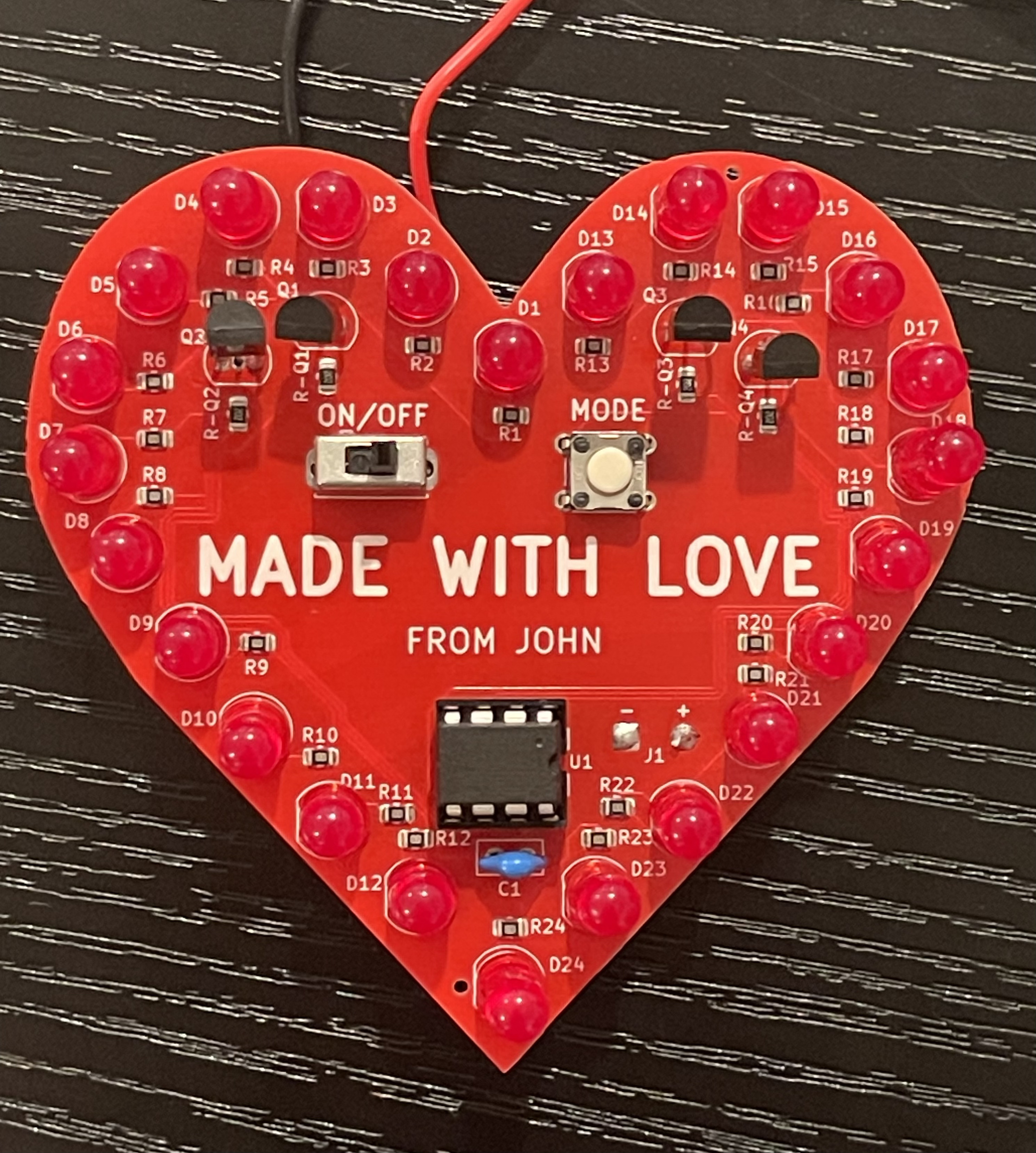
Watch the LED animation demo on YouTube
The MODE button cycles through five lighting patterns:
The 24 LEDs are split into four groups. Each group is switched by an NPN transistor controlled by one ATtiny85 GPIO pin.
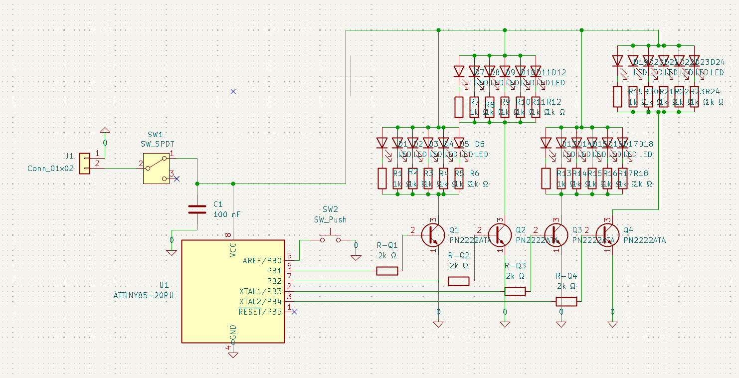
PB0 is connected to the MODE button using the ATtiny85's internal pull-up resistor. PB1–PB4 control the four transistor-switched LED groups.
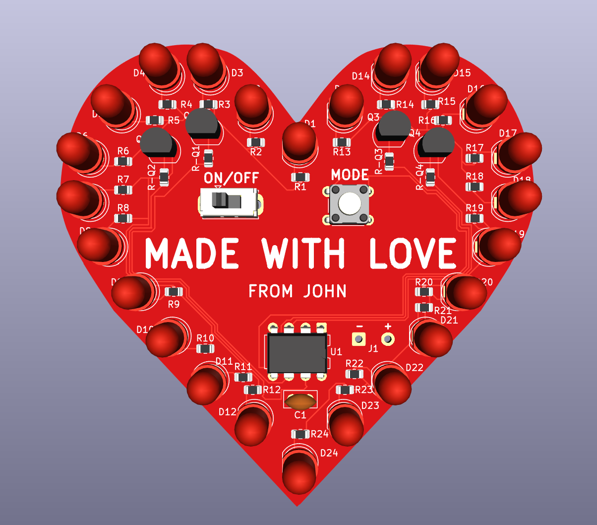
The board was designed in KiCad as a custom 2-layer heart-shaped PCB with a red solder mask and white silkscreen.

The firmware is written in Arduino C/C++ for the ATtiny85 and is available in firmware/attiny85_heartpcb_v1.ino.
The MODE button uses the ATtiny85's PB0 pin-change interrupt. The ISR only sets a flag, while the main loop handles debouncing and mode changes.
All animation timing is non-blocking and uses millis() rather than delay(). Each animation keeps track of its own state so the board can respond to button presses while an animation is running.
The ATtiny85 is configured to use its internal 1 MHz clock.
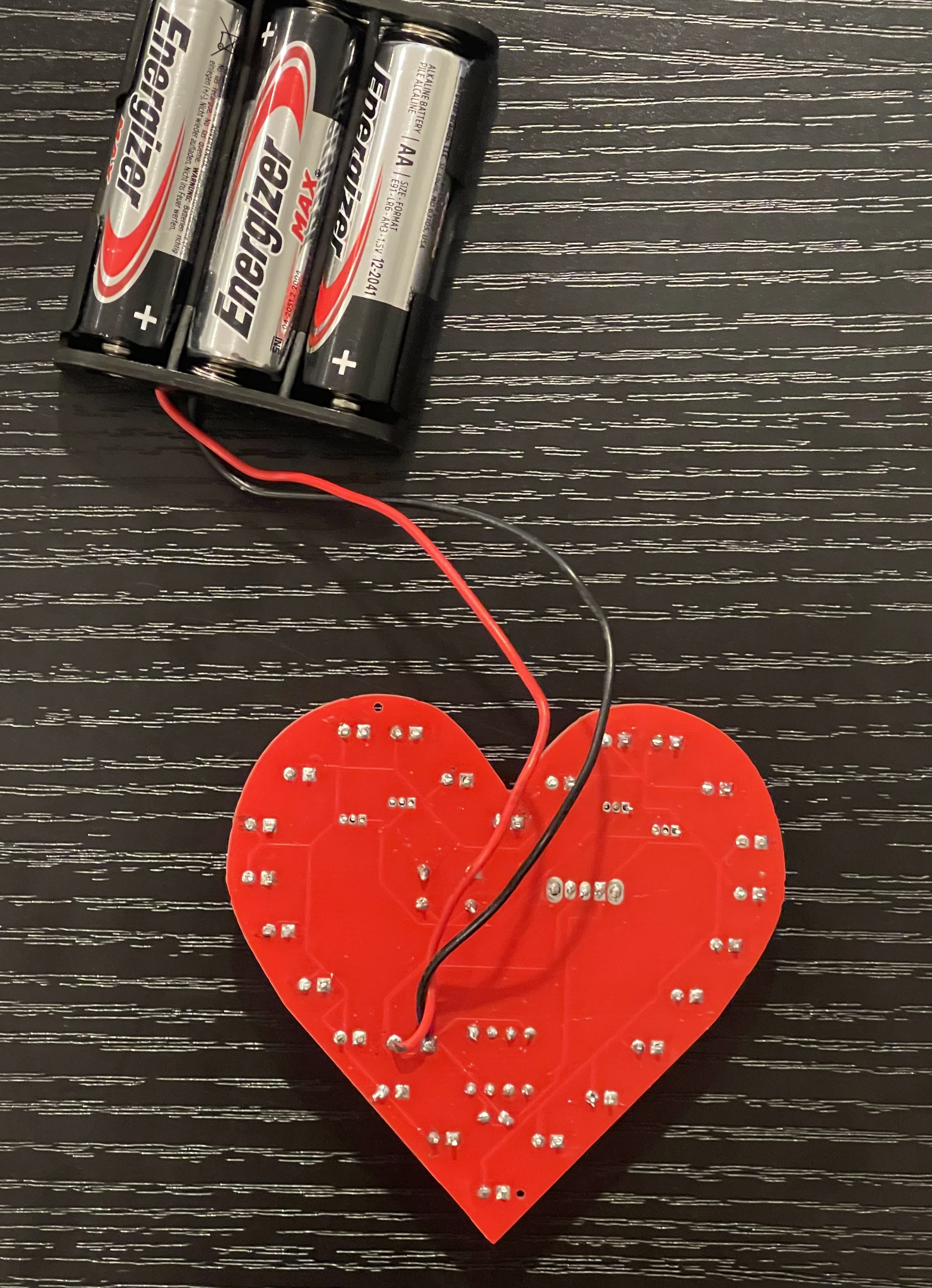
The PCB was fabricated by JLCPCB. The surface-mount resistors were populated through PCBA, while the through-hole LEDs, transistors, ATtiny85 socket, switch, pushbutton, capacitor, and battery wiring were assembled by hand.
The repository also includes the KiCad project files:
hardware/heart_pcb_v1.kicad_prohardware/heart_pcb_v1.kicad_schhardware/heart_pcb_v1.kicad_pcbThis project covered the full workflow from circuit design through a working physical board:
millis()One of the biggest lessons from V1 was designing for assembly and reliability. The through-hole TO-92 transistors were difficult to solder and rework because of the tight lead spacing. A future V2 will likely move more of the design to surface-mount parts, including SMD transistors and LEDs, so most of the board can be assembled directly by the manufacturer.
ATtiny85-Heart-PCB/
├── README.md
├── firmware/
│   └── attiny85_heartpcb_v1.ino
├── hardware/
│   ├── heart_pcb_v1.kicad_pro
│   ├── heart_pcb_v1.kicad_sch
│   ├── heart_pcb_v1.kicad_pcb
│   └── heart_pcb_v1.kicad_prl
└── images/
    ├── heart_pcb_front.jpg
    ├── heart_pcb_back.jpg
    ├── pcb_3d.png
    ├── pcb_layout.png
└── schematic.png| Qty | Value | Footprint | References |
|---|---|---|---|
| 24 | 1k Ω | Resistor_SMD:R_0805_2012Metric | R1, R2, R10, R11, R12, R13, R14, R15, R16, R17, R18, R19, R20, R21, R22, R23 +8 |
| 24 | LED | LED_THT:LED_D5.0mm | D1, D2, D10, D11, D12, D13, D14, D15, D16, D17, D18, D19, D20, D21, D22, D23 +8 |
| 4 | 2k Ω | Resistor_SMD:R_0805_2012Metric | R-Q1, R-Q2, R-Q3, R-Q4 |
| 4 | PN2222ATA | Package_TO_SOT_THT:TO-92_Inline | Q1, Q2, Q3, Q4 |
| 1 | 100 nF | Capacitor_THT:C_Disc_D5.0mm_W2.5mm_P2.50mm | C1 |
| 1 | ATTINY85-20PU | Package_DIP:DIP-8_W7.62mm | U1 |
| 1 | Conn_01x02 | Connector_Wire:SolderWire-0.5sqmm_1x02_P4.6mm_D0.9mm_OD2.1mm | J1 |
| 1 | SW_Push | Button_Switch_THT:SW_TH_Tactile_Omron_B3F-100x | SW2 |
| 1 | SW_SPDT | Button_Switch_THT:SW_Slide_SPDT_Straight_CK_OS102011MS2Q | SW1 |
bwack/C64-Switchless-Multi-Kernal-27C256-adapter
Kernal switcher for the C64/C64C/C128

plusvic/simplebus2-intercom
General description of the Simplebus2 protocol used by some Comelit's intercoms. Hardware for retransmitting Simplebus2 messages over UART.

osmocom/osmocom-analog
Software Implementation of analog cellular telephony systems like NMT, TACS, IMTS, A/B/C-Netz; mirror of https://gitea.osmocom.org/cellular-infrastructure/osmocom-analog

strickyak/jerboa-attiny85-mod-synth
Modular Synthesizer using an ATtiny85 chip for each module.


Hack-a-Day/Remoticon_KiCad_Blender
support files for the 2020 Remoticon KiCad to Blender > PCB renders workshop

It measures 75 × 73.5 mm and has 2 copper layers, 1.6 mm thick.
61 parts, built around the ATTINY85-20PU and PN2222ATA. The full list of its parts is on this page, with links to each part's symbol and footprint where PCBKit's library has them.
From the johnanddd/ATtiny85-Heart-PCB repository on GitHub, at the commit this page was made from: the board is hardware/heart_pcb_v1.kicad_pcb and its schematic hardware/heart_pcb_v1.kicad_sch. PCBKit opens the board in the browser, with nothing to install.
Its repository states no licence, so its author keeps all rights: ask johnanddd before reusing the design.