4 layers160 × 100 mm
Rosco m68k
rosco-m68k/rosco_m68k
Design, documentation and software for the Really Old School Computer (M68K)
140 parts200
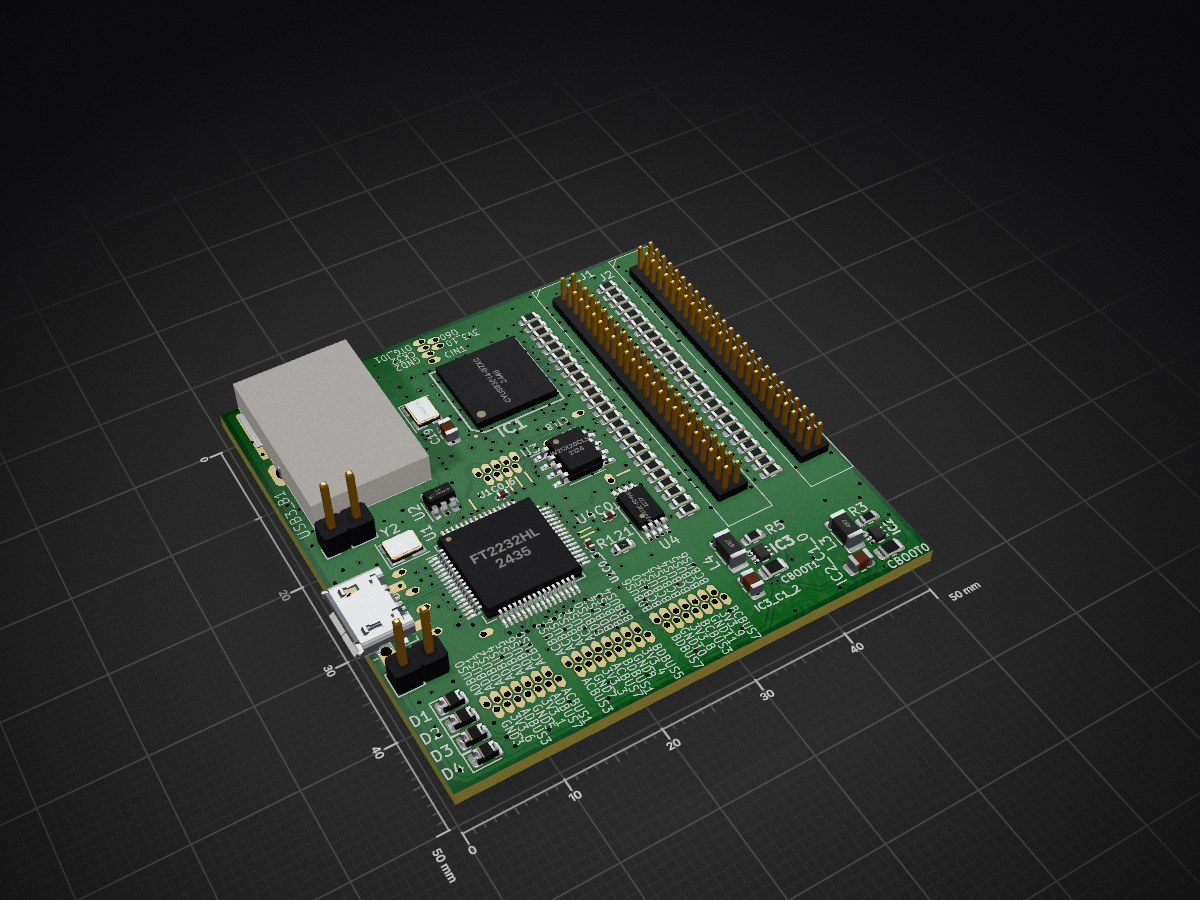
 jkmunson/EENG490
Ez usb dev board is an open-source printed circuit board by jkmunson, from the jkmunson/EENG490 repository on GitHub. It is an 8-layer board of 50 × 50 mm with 287 parts on 219 nets, routed with 2,500 tracks and 661 vias.
It is built around the CYUSB3014-BZXC, W25X20CLSNIG and 93LC56BT-I/OT, with the FT2232HL and M24512E-FDW6TP among its other parts. Its parts include 121 resistors, 50 capacitors, 8 inductors, 7 ICs and 4 diodes. It belongs with the microcontroller boards boards of this library.


| Qty | Value | Footprint | References |
|---|---|---|---|
| 67 | ~ | footprints:tht_testpt_mini | 3V3_1, 3V3_3, 3V3_4, 3V3_6, 3V3_7, 3V3_8, 3V3_9, 3V3_10, ACBUS0, ACBUS1, ACBUS2, ACBUS3, ACBUS4, ACBUS5, ACBUS6, ACBUS7 +51 |
| 50 | match | footprints:R_0603_tight | R13, R14, R15, R16, R17, R18, R19, R20, R21, R22, R23, R24, R25, R26, R27, R28 +34 |
| 50 | terminate | footprints:R_0603_tight | R63, R64, R65, R100, R101, R102, R103, R104, R105, R106, R107, R108, R109, R110, R111, R112 +34 |
| 15 | 2.2uF | Capacitor_SMD:C_0402_1005Metric | C5, C24, U1C0_1, U1C0_2, U1C0_3, U1C0_4, U1C0_5, U1C0_6, U1C0_7, U1C0_8, U1C0_9, U1C0_10, U1C0_11, U3C0_1, U4C0_2 |
| 14 | .1u | Capacitor_SMD:C_0201_0603Metric | C9, C10, C11, C12, C13, C14, C15, C16, C17, C20, C22, C25, C32, C34 |
| 8 | ~ | footprints:trace_tie | NT1, NT2, NT3, NT4, NT5, NT6, NT7, NT8 |
| 7 | 10uF | Capacitor_SMD:C_0805_2012Metric | C26, IC2_C1_0, IC2_C1_1, IC3_C1_2, IC3_C1_3, U1C1_1, U1C1_2 |
| 6 | 100n | Capacitor_SMD:C_0201_0603Metric | C23, C27, C28, C29, C30, C31 |
| 6 | 10k 1% | Resistor_SMD:R_0603_1608Metric | R1, R2, R4, R5, R6, R117 |
| 5 | ~ | Jumper:SolderJumper-3_P2.0mm_Open_TrianglePad1.0x1.5mm | PMOD_0, PMOD_1, PMOD_2, RST_PUL1, RST_SHRT1 |
| 4 | 10k | Resistor_SMD:R_0603_1608Metric | R118, R119, R120, R121 |
| 4 | 10pf C0G 1% | Capacitor_SMD:C_0402_1005Metric | C1, C2, C3, C4 |
| 4 | 1k | Resistor_SMD:R_0805_2012Metric | R9, R10, R11, R12 |
| 4 | 600/.1 2A | Inductor_SMD:L_0805_2012Metric | L5, L6, L7, L8 |
| 4 | LED_Small | Diode_SMD:D_0805_2012Metric | D1, D2, D3, D4 |
| 4 | ~ | Jumper:SolderJumper-2_P1.3mm_Open_TrianglePad1.0x1.5mm | FSLC_0, FSLC_1, FSLC_2, TEST1 |
| 3 | 47uF | Capacitor_SMD:C_0805_2012Metric | C8, C19, C21 |
| 2 | 100n | Resistor_SMD:R_0805_2012Metric | CBOOT0, CBOOT1 |
| 2 | 10k | Resistor_SMD:R_Array_Concave_4x0603 | RN1, RN2 |
| 2 | 2k | Resistor_SMD:R_0603_1608Metric | R115, R116 |
| 2 | 4R7 | Inductor_SMD:L_1206_3216Metric | L3, L4 |
| 2 | 600ac/1dc 100ma | Inductor_SMD:L_0402_1005Metric | L1, L2 |
| 2 | TPS562231DRLR | footprints:SOTFL50P160X60-6N | IC2, IC3 |
| 2 | V5_SEL | Connector_PinHeader_2.54mm:PinHeader_1x02_P2.54mm_Vertical | V5_SEL_3.0B1, V5_SEL_MICRO1 |
| 2 | ~ | footprints:IDCHeader_2x25_spaced | J1, J2 |
| 1 | 12Mhz 10ppm | Crystal:Crystal_SMD_3225-4Pin_3.2x2.5mm | Y2 |
| 1 | 12k/1% | Resistor_SMD:R_0603_1608Metric | R7 |
| 1 | 19.2Mhz | Crystal:Crystal_SMD_3225-4Pin_3.2x2.5mm | Y1 |
| 1 | 2.2u | Capacitor_SMD:C_0402_1005Metric | C18 |
| 1 | 200/1% | Resistor_SMD:R_0603_1608Metric | R114 |
| 1 | 2k | Resistor_SMD:R_1206_3216Metric | R8 |
| 1 | 45.3k 1% | Resistor_SMD:R_0603_1608Metric | R3 |
| 1 | 6.04k/1% | Resistor_SMD:R_0603_1608Metric | R113 |
| 1 | 93LC56BT-I/OT | Package_TO_SOT_SMD:SOT-23-6 | U2 |
| 1 | CYUSB3014-BZXC | footprints:BGA121C80P11X11_1000X1000X120 | IC1 |
| 1 | FT2232HL | Package_QFP:LQFP-64_10x10mm_P0.5mm | U1 |
| 1 | M24512E-FDW6TP | Package_SO:TSSOP-8_4.4x3mm_P0.65mm | U4 |
| 1 | USB3_B | footprints:USB3_B | USB3_B1 |
| 1 | W25X20CLSN | Package_SO:SOIC-8_3.9x4.9mm_P1.27mm | U3 |
| 1 | ~ | Button_Switch_SMD:SW_SPST_EVPBF | SW1 |
| 1 | ~ | footprints:USB_Micro-B_roundholes | MICRO_USB1 |
It measures 50 × 50 mm and has 8 copper layers, 1.62 mm thick.
287 parts, built around the CYUSB3014-BZXC, W25X20CLSNIG, 93LC56BT-I/OT and FT2232HL. The full list of its parts is on this page, with links to each part's symbol and footprint where PCBKit's library has them.
From the jkmunson/EENG490 repository on GitHub, at the commit this page was made from: the board is ez_usb_dev_board/ez_usb_dev_board.kicad_pcb and its schematic analog_tile/analog_tile/analog_tile.kicad_sch. PCBKit opens the board in the browser, with nothing to install.
Its repository states no licence, so its author keeps all rights: ask jkmunson before reusing the design.
rosco-m68k/rosco_m68k
Design, documentation and software for the Really Old School Computer (M68K)


JackToaster/framework_logic_analyzer
16 channel USB 3 Logic analyzer expansion card for Framework laptop